- 您現(xiàn)在的位置:買賣IC網(wǎng) > PDF目錄360914 > IQX320-15PP391 User Programmable Special Function ASIC PDF資料下載
參數(shù)資料
| 型號(hào): | IQX320-15PP391 |
| 英文描述: | User Programmable Special Function ASIC |
| 中文描述: | 用戶可編程ASIC的特殊功能 |
| 文件頁數(shù): | 10/65頁 |
| 文件大小: | 620K |
| 代理商: | IQX320-15PP391 |
第1頁第2頁第3頁第4頁第5頁第6頁第7頁第8頁第9頁當(dāng)前第10頁第11頁第12頁第13頁第14頁第15頁第16頁第17頁第18頁第19頁第20頁第21頁第22頁第23頁第24頁第25頁第26頁第27頁第28頁第29頁第30頁第31頁第32頁第33頁第34頁第35頁第36頁第37頁第38頁第39頁第40頁第41頁第42頁第43頁第44頁第45頁第46頁第47頁第48頁第49頁第50頁第51頁第52頁第53頁第54頁第55頁第56頁第57頁第58頁第59頁第60頁第61頁第62頁第63頁第64頁第65頁
IQX Family Data Sheet
10
Revision 5.0
June 2000
Figure 3. Switch Matrix Control
1.2 Programmable I/O Port
Each signal line in the Switch Matrix is connected to a
programmable I/O Port. The functional attributes of individual I/O
Ports can be programmed independently. The I/O Port attributes
include its signal direction (in, out or bidirectional), data flow
mode (flow-through, registered or latched), and pull-up current.
Figure 4 shows the structure of the programmable I/O Port. The
sources for the four control signals: clock (CLK), clock enable
(CKE), input enable (IE), and output enable (OE) are also
programmable and are described later in the section “I/O Control
Signals.”
Figure 4. Programmable I/O Port
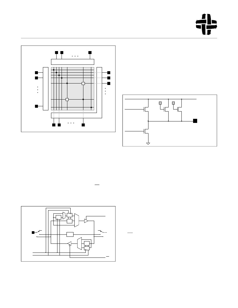
1.2.1 Programmable Pull-up Current
As shown in Figure 5, the I/O Port contains several n-channel
pull-up devices. The normal pull-up current is supplied by a
device which is switched on/off by internally generated control
signal.
An additional
static
pull-up current (I
PU-WK
) or (I
PU-SG
) can be
programmed at each I/O Port pin. This additional pull-up current
is primarily used for but not restricted to the Bus Repeater (BR)
mode.
Figure 5. IQX Output Driver and Pull-Up Current
1.2.2 Pin and Array Side Trickle Current
N-channel devices are used as a trickle current source
(nomnally 10μA) on the pin side and array side for each I/O
Port. Upon reset, these current sources are turned ON. They
can be turned OFF by configuring the I/O Port.
1.2.3 I/O Port Functional Mode
Table 1 describes the various modes of the I/O Port and the
specification used by the I-Cube Development SystemSoftware
for proper bit streamgeneration.
Legend:
Ax -Switch Matrix Signal
Px -I/O Port Signal
IE -Input Enable
OE -Output Enable
CLK -Clock
CKE - Clock Enable
Column (bit) Address Decoder
R
I/O Port Buffers
I
RA
0
RA
1
RA
m-1
CA
0
CA
1
CA
m-1
Row (word)
Address
Column (bit)
Address
P
i
P
j
(j, i)
(i, j)
I/O Port
BR
CLK
CKE
IE
OE
REG
LAT
REG
E
E
E
E
Delay
E
LAT
CK
Switch
Matrix
CK
NC
NC
PU
PD
A)Pull Down
B)Normal Pull Up
C)Additional Weak Pullup
D)Additional Strong Pullup
D
C
A
B
VDD.PAD
I/O Port
Powered by ICminer.com Electronic-Library Service CopyRight 2003
相關(guān)PDF資料 |
PDF描述 |
|---|---|
| IQX320-15PP391I | User Programmable Special Function ASIC |
| IQX320-7PP391 | User Programmable Special Function ASIC |
| IQX320-PB416 | User Programmable Special Function ASIC |
| IR00 | ASIC |
| IR01HD224-P2 | PERIPHERAL DRIVER|1 DRIVER|CMOS|SIP|9PIN|PLASTIC |
相關(guān)代理商/技術(shù)參數(shù) |
參數(shù)描述 |
|---|---|
| IQXO-22C-24.0 | 制造商:IQD Frequency Products 功能描述:OSCILLATOR CRYSTAL |
| IQXO-22C-32MHZ | 制造商:IQD Frequency Products 功能描述:OSCILLATOR CRYSTAL |
| IQXO-22C-4.0 | 制造商:IQD Frequency Products 功能描述:OSCILLATOR CRYSTAL |
| IQXO-22C-50.0 | 制造商:IQD Frequency Products 功能描述:OSCILLATOR CRYSTAL |
| IQXO-331-100.0MHz | 制造商:IQD Frequency Products 功能描述:CRYSTAL OSCILLATOR 100.000000MHZ |
發(fā)布緊急采購,3分鐘左右您將得到回復(fù)。