- 您現在的位置:買賣IC網 > PDF目錄360907 > IPM6220CB Analog IC PDF資料下載
參數資料
| 型號: | IPM6220CB |
| 英文描述: | Analog IC |
| 中文描述: | 模擬IC |
| 文件頁數: | 3/15頁 |
| 文件大小: | 343K |
| 代理商: | IPM6220CB |
3
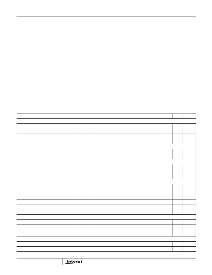
Absolute Maximum Ratings
Thermal Information
Supply Voltage, V
CC
. . . . . . . . . . . . . . . . . . . . . . . . . . . . . . . . +6.5V
Input Voltage, V
IN
. . . . . . . . . . . . . . . . . . . . . . . . . . . . . . . . . . +27.0V
V3in . . . . . . . . . . . . . . . . . . . . . . . . . . . . . . . . . . . . . . . . . . . . . +6.5V
PHASE1,2 . . . . . . . . . . . . . . . . . . . . . . . . . . . . . . . . . . . . . . . +33.0V
BOOT1,2 . . . . . . . . . . . . . . . . . . . . . . . . . . . . . . . . . . . . . . . . +33.0V
BOOT1,2 with respect to PHASE1,2 . . . . . . . . . . . . . . . . . . . . . +6.5V
PGOOD, RT/FAULT, and GATE Voltage . . . .GND - 0.3V to V
CC
+0.3V
Core Output or I/O Voltage . . . . . . . . . . . . . . . GND - 0.3V to +6.5V
ESD Classification . . . . . . . . . . . . . . . . . . . . . . . . . . . . . . . . .Class 2
Recommended Operating Conditions
Supply Voltage, V
CC
. . . . . . . . . . . . . . . . . . . . . . . . . . . +5.0V
±
5%
Input Voltage, V
IN
. . . . . . . . . . . . . . . . . . . . . . . . . . . +7.5V to 24.0V
V3in . . . . . . . . . . . . . . . . . . . . . . . . . . . . . . . . . . . . . . . +3.3V
±
10%
Ambient Temperature Range. . . . . . . . . . . . . . . . . . . -10
o
C to 85
o
C
Junction Temperature Range. . . . . . . . . . . . . . . . . . -10
o
C to 125
o
C
Thermal Resistance (Typical, Note 1)
SSOP Package . . . . . . . . . . . . . . . . . . . . . . . . . . . .
Maximum Junction Temperature (Plastic Package) . . . . . . . .150
o
C
Maximum Storage Temperature Range. . . . . . . . . . -65
o
C to 150
o
C
Maximum Lead Temperature (Soldering 10s) . . . . . . . . . . . . .300
o
C
(SSOP - Lead Tips Only)
θ
JA
(
o
C/W)
100
CAUTION: Stresses above those listed in “Absolute Maximum Ratings” may cause permanent damage to the device. This is a stress only rating and operation of the
device at these or any other conditions above those indicated in the operational sections of this specification is not implied.
NOTE:
1.
θ
JA
is measured with the component mounted on a low effective thermal conductivity test board in free air. See Tech Brief TB379 for details.
Electrical Specifications
Recommended Operating Conditions, Unless Otherwise Noted. Refer to Figures 1, 2 and 3
PARAMETER
SYMBOL
TEST CONDITIONS
MIN
TYP
MAX
UNITS
VCC SUPPLY
Nominal Supply Current
I
CC
I
CCS
I
VIN
I
VINSD
GATE1, GATE2 Open
-
2
2.5
mA
Shutdown Supply Current
-
30
-
μ
A
Battery Pin Supply Current
30
-
200
μ
A
Battery Pin Leakage Current at Shutdown
-
-
1
μ
A
POWER-ON RESET
Rising VCC Threshold
4.3
4.5
4.6
V
Falling VCC Threshold
3.9
4.1
4.3
V
OSCILLATOR
Free Running Frequency
255
300
345
kHz
Ramp Amplitude, peak-to-peak
V
BAT
= 16V
-
2
-
V
Ramp Offset
-
0.5
-
V
REFERENCE, DAC AND SOFT START
VID0-VID4 Input Low Voltage
-
-
1.2
V
VID0-VID4 Input High Voltage
1.8
-
-
V
VID0-VID4 Pull-up Current to V
CC
DAC Voltage Accuracy
-
1
-
μ
A
-1.0
-
+1.0
%
Soft-Start Current During Start-Up
I
SS
I
SSM
V
SS
= 0V...0.9V
V
SS
= 0.925V...2.0V
18
25
32
μ
A
Soft-Start Current During Mode Change
350
500
650
μ
A
ENABLE
Enable Voltage Low
V
ENLOW
V
ENHIGH
IC Inhibited
-
-
1.2
V
Enable Voltage High
IC Enabled
Input has Internal Pull-up Current Source 2
μ
A
(Typ)
2.0
-
-
V
PWM 1 CONVERTER
Output Voltage
VOUT1
Defined by the current VID code (Table 1)
0.925
-
2.0
V
Static Load Regulation
100mA < I
VOUT1
< 15.0A
-2.0
-
+2.0
%
IPM6210
相關PDF資料 |
PDF描述 |
|---|---|
| IPM6210CA | Analog IC |
| IPS0551T(SMD220) | TRANSISTOR | MOSFET | N-CHANNEL | 37V V(BR)DSS | TO-273VAR |
| IPS0551T(TO220) | TRANSISTOR | MOSFET | N-CHANNEL | 37V V(BR)DSS | TO-273AA |
| IPS511E | PERIPHERAL DRIVER|1 DRIVER|MOS|LLCC|18PIN|CERAMIC |
| IPS5551T(SMD220) | PERIPHERAL DRIVER|1 DRIVER|MOS|SIP|3PIN|PLASTIC |
相關代理商/技術參數 |
參數描述 |
|---|---|
| IPM6220EVAL1 | 制造商:INTERSIL 制造商全稱:Intersil Corporation 功能描述:Advanced Triple PWM Only Mode and Dual Linear Power Controller for Portable Applications |
| IPM-C112 | 制造商:JDSU 制造商全稱:JDS Uniphase Corporation 功能描述:Miniature Integrated Power Monitor |
| IPM-C113 | 制造商:JDSU 制造商全稱:JDS Uniphase Corporation 功能描述:Miniature Integrated Power Monitor |
| IPM-C114 | 制造商:JDSU 制造商全稱:JDS Uniphase Corporation 功能描述:Miniature Integrated Power Monitor |
| IPM-C122 | 制造商:JDSU 制造商全稱:JDS Uniphase Corporation 功能描述:Miniature Integrated Power Monitor |
發(fā)布緊急采購,3分鐘左右您將得到回復。