- 您現(xiàn)在的位置:買賣IC網(wǎng) > PDF目錄67714 > IDT74FCT88915TT70PY8 (INTEGRATED DEVICE TECHNOLOGY INC) FCT SERIES, PLL BASED CLOCK DRIVER, 7 TRUE OUTPUT(S), 1 INVERTED OUTPUT(S), PDSO28 PDF資料下載
參數(shù)資料
| 型號(hào): | IDT74FCT88915TT70PY8 |
| 廠商: | INTEGRATED DEVICE TECHNOLOGY INC |
| 元件分類: | 時(shí)鐘及定時(shí) |
| 英文描述: | FCT SERIES, PLL BASED CLOCK DRIVER, 7 TRUE OUTPUT(S), 1 INVERTED OUTPUT(S), PDSO28 |
| 封裝: | SSOP-28 |
| 文件頁(yè)數(shù): | 5/11頁(yè) |
| 文件大小: | 108K |
| 代理商: | IDT74FCT88915TT70PY8 |
3
IDT74FCT88915TT
LOW SKEW PLL-BASED CMOS CLOCK DRIVER
COMMERCIALTEMPERATURERANGE
NOTES:
1. Stresses greater than those listed under ABSOLUTE MAXIMUM RATINGS may cause
permanent damage to the device. This is a stress rating only and functional operation
of the device at these or any other conditions above those indicated in the operational
sections of this specification is not implied. Exposure to absolute maximum rating
conditions for extended periods may affect reliability. No terminal voltage may exceed
VCC by +0.5V unless otherwise noted.
2. Input and VCC terminals.
3. Outputs and I/O terminals.
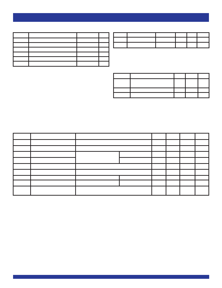
ABSOLUTE MAXIMUM RATINGS(1)
(1)
Symbol
Description
Max.
Unit
VTERM(2)
Terminal Voltage with Respect to GND
–0.5 to 7
V
VTERM(3)
Terminal Voltage with Respect to GND
–0.5 to VCC+0.5
V
TA
OperatingTemperature
0 to +70
° C
TBIAS
TemperatureUnderBias
–55 to +125
° C
TSTG
StorageTemperature
–55 to +125
° C
IOUT
DC Output Current
–60 to 120
mA
Symbol
Parameter
(1)
Conditions
Typ.
Max.
Unit
CIN
Input Capacitance
VIN = 0V
4.5
6
pF
COUT
Output Capacitance
VOUT = 0V
5.5
8
pF
CAPACITANCE (TA= +25°C,f=1.0MHz)
NOTE:
1. This parameter is measured at characterization but not tested.
Symbol
Parameter
Min.
Max.
Unit
TRISE/FALL
Rise/Fall Times, SYNC inputs
—
3
ns
(0.8V to 2.0V)
Frequency
Input Frequency, SYNC Inputs
10
2Q fmax
MHz
Duty Cycle
Input Duty Cycle, SYNC Inputs
25%
75%
—
SYNC INPUT TIMING REQUIREMENTS
Symbol
Parameter
Test Conditions(1)
Min.
Typ.(2)
Max.
Unit
VIH
Input HIGH Level
Guaranteed Logic HIGH Level
2
—
V
VIL
Input LOW Level
Guaranteed Logic LOW Level
—
0.8
V
IIH
Input HIGH Current
VCC = Max.
VI = VCC
——
±1 A
IIL
Input LOW Current
VI = GND
—
±1 A
VIK
Clamp Diode Voltage
VCC = Min., IIN = –18mA
—
–0.7
–1.2
V
VIH
Input Hysteresis
—
100
—
mV
VOH
Output HIGH Voltage
VCC = Min.
IOH = –15mA
2.4
3.5
—
V
VOL
Output LOW Voltage
VCC = Min.
IOL = 64mA
—
0.2
0.55
V
ICCL
Quiescent Power Supply Current
VCC = Max., VIN = GND or VCC
—2
4
mA
ICCH
(Test mode, LF connected to GND)
DC ELECTRICAL CHARACTERISTICS OVER OPERATING RANGE
Following Conditions Apply Unless Otherwise Specified:
Commercial: TA = 0°C to 70°C, VCC = 5.0V ±5%
NOTES:
1. For conditions shown as Min. or Max., use appropriate value specified under Electrical Characteristics for the applicable device type.
2. Typical values are at VCC = 5.0V, +25°C ambient.
3. Not more than one output should be tested at one time. Duration of the test should not exceed one second.
相關(guān)PDF資料 |
PDF描述 |
|---|---|
| IDT74SSTU32864GBF | SSTU SERIES, POSITIVE EDGE TRIGGERED D FLIP-FLOP, TRUE OUTPUT, PBGA96 |
| IDT74SSTU32864CBF8 | SSTU SERIES, POSITIVE EDGE TRIGGERED D FLIP-FLOP, TRUE OUTPUT, PBGA96 |
| IDT74SSTU32864GBFG | SSTU SERIES, POSITIVE EDGE TRIGGERED D FLIP-FLOP, TRUE OUTPUT, PBGA96 |
| IDT74SSTU32864ABFG8 | SSTU SERIES, POSITIVE EDGE TRIGGERED D FLIP-FLOP, TRUE OUTPUT, PBGA96 |
| IDT74SSTU32864CBF | SSTU SERIES, POSITIVE EDGE TRIGGERED D FLIP-FLOP, TRUE OUTPUT, PBGA96 |
相關(guān)代理商/技術(shù)參數(shù) |
參數(shù)描述 |
|---|---|
| IDT74FST163211PV | 制造商:Integrated Device Technology Inc 功能描述: |
| IDT74FST163233PV | 制造商:Integrated Device Technology Inc 功能描述: |
| IDT74FST16323PA | 制造商:Integrated Device Technology Inc 功能描述: |
| IDT74FST163244DPF | 制造商:Rochester Electronics LLC 功能描述:- Bulk 制造商:Integrated Device Technology Inc 功能描述: |
| IDT74FST163244PA | 制造商:INT_DEV_TECH 功能描述: |
發(fā)布緊急采購(gòu),3分鐘左右您將得到回復(fù)。