- 您現(xiàn)在的位置:買賣IC網(wǎng) > PDF目錄9968 > IDT72V3654L15PF (IDT, Integrated Device Technology Inc)IC BI FIFO 4096X36 15NS 128QFP PDF資料下載
參數(shù)資料
| 型號(hào): | IDT72V3654L15PF |
| 廠商: | IDT, Integrated Device Technology Inc |
| 文件頁數(shù): | 16/37頁 |
| 文件大?。?/td> | 0K |
| 描述: | IC BI FIFO 4096X36 15NS 128QFP |
| 標(biāo)準(zhǔn)包裝: | 36 |
| 系列: | 72V |
| 功能: | 異步 |
| 存儲(chǔ)容量: | 147K(4K x 36) |
| 數(shù)據(jù)速率: | 67MHz |
| 訪問時(shí)間: | 15ns |
| 電源電壓: | 3.15 V ~ 3.45 V |
| 工作溫度: | 0°C ~ 70°C |
| 安裝類型: | 表面貼裝 |
| 封裝/外殼: | 128-LQFP |
| 供應(yīng)商設(shè)備封裝: | 128-TQFP(14x20) |
| 包裝: | 托盤 |
| 其它名稱: | 72V3654L15PF |
第1頁第2頁第3頁第4頁第5頁第6頁第7頁第8頁第9頁第10頁第11頁第12頁第13頁第14頁第15頁當(dāng)前第16頁第17頁第18頁第19頁第20頁第21頁第22頁第23頁第24頁第25頁第26頁第27頁第28頁第29頁第30頁第31頁第32頁第33頁第34頁第35頁第36頁第37頁
23
COMMERCIALTEMPERATURERANGE
IDT72V3654/72V3664/72V3674 3.3V CMOS SyncBiFIFOTM WITH BUS-MATCHING
2,048 x 36 x 2, 4,096 x 36 x 2 and 8,192 x 36 x 2
DATA SIZE TABLE FOR BYTE READS FROM FIFO1
SIZE MODE(1)
DATA WRITTEN TO FIFO1
READ
DATA READ FROM FIFO1
NO.
BM
SIZE
BE
A35-A27
A26-A18
A17-A9
A8-A0
B8-B0
HH
H
A
B
C
D
HH
L
A
B
C
D
1
A
2
B
3
C
4
D
1
D
2
C
3
B
4
A
NOTE:
1. BE is selected at Master Reset; BM and SIZE must be static throughout device operation.
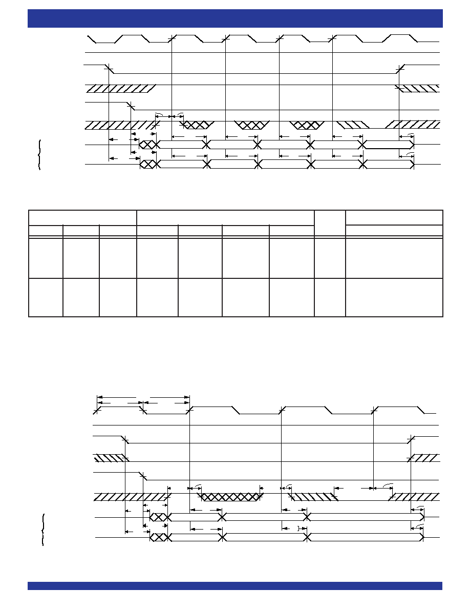
Figure 13. Port-B Byte Read Cycle Timing for FIFO1 (IDT Standard and FWFT Modes)
Figure 14. Port-A Read Cycle Timing for FIFO2 (IDT Standard and FWFT Modes)
NOTE:
1. Unused bytes B9-B17, B18-B26, and B27-B35 are indeterminate for byte-size reads.
NOTE:
1. Read From FIFO2.
EFB/ORB
MBB
CSB
W/RB
ENB
CLKB
HIGH
B0-B8
Read 5
Read 2
Read 3
Read 4
Read 3
Read 4
Previous Data
Read 2
No Operation
tDIS
tA
tENS2
tENH
tA
Read 1
(Standard Mode)
(FWFT Mode)
tEN
tMDV
tEN
OR
Read 1
4664 drw 15
4664 drw16
CLKA
EFA/ORA
ENA
MBA
CSA
W/RA
tCLK
tCLKH
tCLKL
tENS2
tA
tMDV
tEN
tA
tENS2
tENH
tENS2
tENH
W1
W2
W3
(1)
tENH
tDIS
No Operation
A0-A35
(FWFT Mode)
tEN
W2
(1)
tDIS
W1
Previous Data
A0-A35
(Standard Mode)
tMDV
tA
OR
tA
HIGH
(1)
相關(guān)PDF資料 |
PDF描述 |
|---|---|
| V48B12M250BL3 | CONVERTER MOD DC/DC 12V 250W |
| V48B12M250BL | CONVERTER MOD DC/DC 12V 250W |
| IDT72V3653L15PF | IC SYNCFIFO 2048X36 15NS 128TQFP |
| IDT82P2521BH | IC LIU E1 21+1CH SHORT 640-PBGA |
| IDT72V3652L15PQF | IC BI FIFO 4096X36 15NS 132QFP |
相關(guān)代理商/技術(shù)參數(shù) |
參數(shù)描述 |
|---|---|
| IDT72V3654L15PF8 | 功能描述:IC BI FIFO 4096X36 15NS 128QFP RoHS:否 類別:集成電路 (IC) >> 邏輯 - FIFO 系列:72V 標(biāo)準(zhǔn)包裝:90 系列:7200 功能:同步 存儲(chǔ)容量:288K(16K x 18) 數(shù)據(jù)速率:100MHz 訪問時(shí)間:10ns 電源電壓:4.5 V ~ 5.5 V 工作溫度:0°C ~ 70°C 安裝類型:表面貼裝 封裝/外殼:64-LQFP 供應(yīng)商設(shè)備封裝:64-TQFP(14x14) 包裝:托盤 其它名稱:72271LA10PF |
| IDT72V3656L10PF | 功能描述:IC SYNC FIFO 4096X36 10NS 128QFP RoHS:否 類別:集成電路 (IC) >> 邏輯 - FIFO 系列:72V 標(biāo)準(zhǔn)包裝:90 系列:7200 功能:同步 存儲(chǔ)容量:288K(16K x 18) 數(shù)據(jù)速率:100MHz 訪問時(shí)間:10ns 電源電壓:4.5 V ~ 5.5 V 工作溫度:0°C ~ 70°C 安裝類型:表面貼裝 封裝/外殼:64-LQFP 供應(yīng)商設(shè)備封裝:64-TQFP(14x14) 包裝:托盤 其它名稱:72271LA10PF |
| IDT72V3656L10PF8 | 功能描述:IC SYNC FIFO 4096X36 10NS 128QFP RoHS:否 類別:集成電路 (IC) >> 邏輯 - FIFO 系列:72V 標(biāo)準(zhǔn)包裝:90 系列:7200 功能:同步 存儲(chǔ)容量:288K(16K x 18) 數(shù)據(jù)速率:100MHz 訪問時(shí)間:10ns 電源電壓:4.5 V ~ 5.5 V 工作溫度:0°C ~ 70°C 安裝類型:表面貼裝 封裝/外殼:64-LQFP 供應(yīng)商設(shè)備封裝:64-TQFP(14x14) 包裝:托盤 其它名稱:72271LA10PF |
| IDT72V3656L10PFI | 制造商:Integrated Device Technology Inc 功能描述:IC SYNC FIFO 4096X36 10NS 128QFP |
| IDT72V3656L10PFI8 | 制造商:Integrated Device Technology Inc 功能描述:IC SYNC FIFO 4096X36 10NS 128QFP |
發(fā)布緊急采購,3分鐘左右您將得到回復(fù)。