- 您現(xiàn)在的位置:買賣IC網(wǎng) > PDF目錄9968 > IDT72V3654L15PF (IDT, Integrated Device Technology Inc)IC BI FIFO 4096X36 15NS 128QFP PDF資料下載
參數(shù)資料
| 型號(hào): | IDT72V3654L15PF |
| 廠商: | IDT, Integrated Device Technology Inc |
| 文件頁數(shù): | 11/37頁 |
| 文件大小: | 0K |
| 描述: | IC BI FIFO 4096X36 15NS 128QFP |
| 標(biāo)準(zhǔn)包裝: | 36 |
| 系列: | 72V |
| 功能: | 異步 |
| 存儲(chǔ)容量: | 147K(4K x 36) |
| 數(shù)據(jù)速率: | 67MHz |
| 訪問時(shí)間: | 15ns |
| 電源電壓: | 3.15 V ~ 3.45 V |
| 工作溫度: | 0°C ~ 70°C |
| 安裝類型: | 表面貼裝 |
| 封裝/外殼: | 128-LQFP |
| 供應(yīng)商設(shè)備封裝: | 128-TQFP(14x20) |
| 包裝: | 托盤 |
| 其它名稱: | 72V3654L15PF |
第1頁第2頁第3頁第4頁第5頁第6頁第7頁第8頁第9頁第10頁當(dāng)前第11頁第12頁第13頁第14頁第15頁第16頁第17頁第18頁第19頁第20頁第21頁第22頁第23頁第24頁第25頁第26頁第27頁第28頁第29頁第30頁第31頁第32頁第33頁第34頁第35頁第36頁第37頁
19
COMMERCIALTEMPERATURERANGE
IDT72V3654/72V3664/72V3674 3.3V CMOS SyncBiFIFOTM WITH BUS-MATCHING
2,048 x 36 x 2, 4,096 x 36 x 2 and 8,192 x 36 x 2
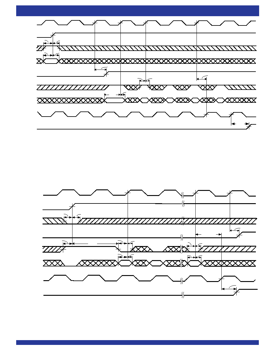
Figure 6. Serial Programming of the Almost-Full Flag and Almost-Empty Flag Offset Values (IDT Standard and FWFT Modes)
Figure 5. Parallel Programming of the Almost-Full Flag and Almost-Empty Flag Offset Values after Reset (IDT Standard and FWFT Modes)
NOTES:
1. tSKEW1 is the minimum time between the rising CLKA edge and a rising CLKB edge for
FFB/IRB to transition HIGH in the next cycle. If the time between the rising edge of CLKA and rising
edge of CLKB is less than tSKEW1, then
FFB/IRB may transition HIGH one CLKB cycle later than shown.
2. It is not necessary to program offset register bits on consecutive clock cycles. FIFO write attempts are ignored until
FFA/IRA and FFB/IRB is set HIGH.
3. Programmable offsets are written serially to the SD input in the order
AFA offset (Y1), AEB offset (X1), AFB offset (Y2), and AEA offset (X2).
NOTES:
1. tSKEW1 is the minimum time between the rising CLKA edge and a rising CLKB edge for
FFB/IRB to transition HIGH in the next cycle. If the time between the rising edge of CLKA and rising
edge of CLKB is less than tSKEW1, then
FFB/IRB may transition HIGH one CLKB cycle later than shown.
2.
CSA=LOW, W/RA=HIGH,MBA=LOW. It is not necessary to program offset register on consecutive clock cycles.
4664 drw 07
CLKA
MRS1,
MRS2
FFA/IRA
CLKB
FFB/IRB
A0-A35
FS1,FS0
ENA
tFSH
tWFF
tENH
tENS2
tSKEW1
tDS
tDH
tWFF
4
0,0
AFA Offset
(Y1)
AEB Offset
(X1)
AFB Offset
(Y 2)
AEA Offset
(X 2)
First Word to FIFO1
12
(1)
tFSH
tFSS
1
2
FS2
CLKA
FFA/IRA
t
tSENH
FS0/SD(3)
tSPH
tSENS
tSENH
tFSS
tWFF
FS1/SEN
AEA Offset (X2) LSB
tSDS
tSDH
tSDS
tSDH
AFA Offset (Y1) MSB
MRS1,
MRS2
4
4664 drw 08
tFSS
tFSH
CLKB
4
FS2
FFB/IRB
tWFF
tSKEW(1)
相關(guān)PDF資料 |
PDF描述 |
|---|---|
| V48B12M250BL3 | CONVERTER MOD DC/DC 12V 250W |
| V48B12M250BL | CONVERTER MOD DC/DC 12V 250W |
| IDT72V3653L15PF | IC SYNCFIFO 2048X36 15NS 128TQFP |
| IDT82P2521BH | IC LIU E1 21+1CH SHORT 640-PBGA |
| IDT72V3652L15PQF | IC BI FIFO 4096X36 15NS 132QFP |
相關(guān)代理商/技術(shù)參數(shù) |
參數(shù)描述 |
|---|---|
| IDT72V3654L15PF8 | 功能描述:IC BI FIFO 4096X36 15NS 128QFP RoHS:否 類別:集成電路 (IC) >> 邏輯 - FIFO 系列:72V 標(biāo)準(zhǔn)包裝:90 系列:7200 功能:同步 存儲(chǔ)容量:288K(16K x 18) 數(shù)據(jù)速率:100MHz 訪問時(shí)間:10ns 電源電壓:4.5 V ~ 5.5 V 工作溫度:0°C ~ 70°C 安裝類型:表面貼裝 封裝/外殼:64-LQFP 供應(yīng)商設(shè)備封裝:64-TQFP(14x14) 包裝:托盤 其它名稱:72271LA10PF |
| IDT72V3656L10PF | 功能描述:IC SYNC FIFO 4096X36 10NS 128QFP RoHS:否 類別:集成電路 (IC) >> 邏輯 - FIFO 系列:72V 標(biāo)準(zhǔn)包裝:90 系列:7200 功能:同步 存儲(chǔ)容量:288K(16K x 18) 數(shù)據(jù)速率:100MHz 訪問時(shí)間:10ns 電源電壓:4.5 V ~ 5.5 V 工作溫度:0°C ~ 70°C 安裝類型:表面貼裝 封裝/外殼:64-LQFP 供應(yīng)商設(shè)備封裝:64-TQFP(14x14) 包裝:托盤 其它名稱:72271LA10PF |
| IDT72V3656L10PF8 | 功能描述:IC SYNC FIFO 4096X36 10NS 128QFP RoHS:否 類別:集成電路 (IC) >> 邏輯 - FIFO 系列:72V 標(biāo)準(zhǔn)包裝:90 系列:7200 功能:同步 存儲(chǔ)容量:288K(16K x 18) 數(shù)據(jù)速率:100MHz 訪問時(shí)間:10ns 電源電壓:4.5 V ~ 5.5 V 工作溫度:0°C ~ 70°C 安裝類型:表面貼裝 封裝/外殼:64-LQFP 供應(yīng)商設(shè)備封裝:64-TQFP(14x14) 包裝:托盤 其它名稱:72271LA10PF |
| IDT72V3656L10PFI | 制造商:Integrated Device Technology Inc 功能描述:IC SYNC FIFO 4096X36 10NS 128QFP |
| IDT72V3656L10PFI8 | 制造商:Integrated Device Technology Inc 功能描述:IC SYNC FIFO 4096X36 10NS 128QFP |
發(fā)布緊急采購(gòu),3分鐘左右您將得到回復(fù)。