- 您現(xiàn)在的位置:買賣IC網(wǎng) > PDF目錄299200 > IDT7005L55PFB (INTEGRATED DEVICE TECHNOLOGY INC) HIGH-SPEED 8K x 8 DUAL-PORT STATIC RAM PDF資料下載
參數(shù)資料
| 型號(hào): | IDT7005L55PFB |
| 廠商: | INTEGRATED DEVICE TECHNOLOGY INC |
| 元件分類: | SRAM |
| 英文描述: | HIGH-SPEED 8K x 8 DUAL-PORT STATIC RAM |
| 中文描述: | 8K X 8 DUAL-PORT SRAM, 55 ns, PQFP64 |
| 封裝: | 14 X 14 MM, 1.40 MM HEIGHT, TQFP-64 |
| 文件頁數(shù): | 18/20頁 |
| 文件大小: | 189K |
| 代理商: | IDT7005L55PFB |
6.42
IDT7005S/L
High-Speed 8K x 8 Dual-Port Static RAM
Military, Industrial and Commercial Temperature Ranges
7
AC Test Conditions
NOTES:
1. Transition is measured 0mV from Low or High impedance voltage with load (Figures 1 and 2).
2. This parameter is guaranteed but not production tested.
3. To access RAM,
CE = VIL and SEM = VIH. To access semaphore, CE = VIH and SEM = VIL.
4. 'X' in part number indicates power rating (S or L).
5. Industrial temperature: for other speeds, packages and powers contact your sales office.
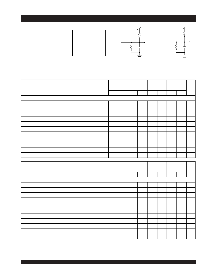
Figure 1. AC Output Test Load
Figure 2. Output Test Load
(For tLZ, tHZ, tWZ, tOW)
*Including scope and jig
AC Electrical Characteristics Over the
Operating Temperature and Supply Voltage Range(4,5)
1250
30pF
775
DATAOUT
BUSY
INT
5V
1250
5pF*
775
DATAOUT
2738 drw 06
Input Pulse Levels
Input Rise/Fall Times
Input Timing Reference Levels
Output Reference Levels
Output Load
GND to 3.0V
5ns Max.
1.5V
Figures 1 and 2
2738 tbl 12
7005X15
Com'l Only
7005X17
Com'l Only
7005X20
Com'l &
Military
7005X25
Com'l &
Military
Unit
Symbol
Parameter
Min.Max.Min.Max.Min.
Max.Min.Max.
READ CYCLE
tRC
Read Cycle Time
15
____
17
____
20
____
25
____
ns
tAA
Address Access Time
____
15
____
17
____
20
____
25
ns
tACE
Chip Enable Access Time(3)
____
15
____
17
____
20
____
25
ns
tAOE
Output Enable Access Time
____
10
____
10
____
12
____
13
ns
tOH
Output Hold from Address Change
3
____
3
____
3
____
3
____
ns
tLZ
Output Low-Z Time(1,2)
3
____
3
____
3
____
3
____
ns
tHZ
Output High-Z Time(1,2)
____
10
____
10
____
12
____
15
ns
tPU
Chip Enable to Power Up Time(2,5)
0
____
0
____
0
____
0
____
ns
tPD
Chip Disable to Power Down Time (2,5)
____
15
____
17
____
20
____
25
ns
tSOP
Semapho re Flag Update Pulse (OE or SEM)
10
____
10
____
10
____
10
____
ns
tSAA
Semaphore Address Access Time
____
15
____
17
____
20
____
25
ns
2738 tbl 13a
7005X35
Com'l, Ind
& Military
7005X55
Com'l, Ind
& Military
IDT7005X70
Military
Only
Unit
Symbol
Parameter
Min.
Max.
Min.
Max.
Min.
Max.
READ CYCLE
tRC
Read Cycle Time
35
____
55
____
70
____
ns
tAA
Address Access Time
____
35
____
55
____
70
ns
tACE
Chip Enable Access Time(3)
____
35
____
55
____
70
ns
tAOE
Output Enable Access Time
____
20
____
30
____
35
ns
tOH
Output Hold from Address Change
3
____
3
____
3
____
ns
tLZ
Output Low-Z Time(1,2)
3
____
3
____
3
____
ns
tHZ
Output High-Z Time(1,2)
____
15
____
25
____
30
ns
tPU
Chip Enab le to Power Up Time(2,5)
0
____
0
____
0
____
ns
tPD
Chip Disable to Power Down Time(2,5)
____
35
____
50
____
50
ns
tSOP
Semaphore Flag Update Pulse (OE or SEM)
15
____
15
____
15
____
ns
tSAA
Semaphore Address Access Time
____
35
____
55
____
70
ns
2738 tbl 13b
相關(guān)PDF資料 |
PDF描述 |
|---|---|
| IDT7005S | HIGH-SPEED 8K x 8 DUAL-PORT STATIC RAM |
| IDT7034L20PF8 | 4K X 18 DUAL-PORT SRAM, 20 ns, PQFP100 |
| IDT709199L12PFG | 128K X 9 DUAL-PORT SRAM, 25 ns, PQFP100 |
| IDT70V34TS20PFI | 4K X 18 DUAL-PORT SRAM, 20 ns, PQFP100 |
| IDT71256L35PI | 32K X 8 STANDARD SRAM, 35 ns, PDIP28 |
相關(guān)代理商/技術(shù)參數(shù) |
參數(shù)描述 |
|---|---|
| IDT7005L55XL | 制造商:未知廠家 制造商全稱:未知廠家 功能描述:x8 Dual-Port SRAM |
| IDT7005L55XLB | 制造商:未知廠家 制造商全稱:未知廠家 功能描述:x8 Dual-Port SRAM |
| IDT7005L70F | 制造商:IDT 制造商全稱:Integrated Device Technology 功能描述:HIGH-SPEED 8K x 8 DUAL-PORT STATIC RAM |
| IDT7005L70FB | 制造商:IDT 制造商全稱:Integrated Device Technology 功能描述:HIGH-SPEED 8K x 8 DUAL-PORT STATIC RAM |
| IDT7005L70G | 制造商:IDT 制造商全稱:Integrated Device Technology 功能描述:HIGH-SPEED 8K x 8 DUAL-PORT STATIC RAM |
發(fā)布緊急采購,3分鐘左右您將得到回復(fù)。