- 您現(xiàn)在的位置:買賣IC網(wǎng) > PDF目錄360786 > ICS950813YGT Frequency Generator with 200MHz Differential CPU Clocks PDF資料下載
參數(shù)資料
| 型號: | ICS950813YGT |
| 英文描述: | Frequency Generator with 200MHz Differential CPU Clocks |
| 中文描述: | 頻率發(fā)生器200MHz的CPU的時鐘差分 |
| 文件頁數(shù): | 7/22頁 |
| 文件大小: | 265K |
| 代理商: | ICS950813YGT |
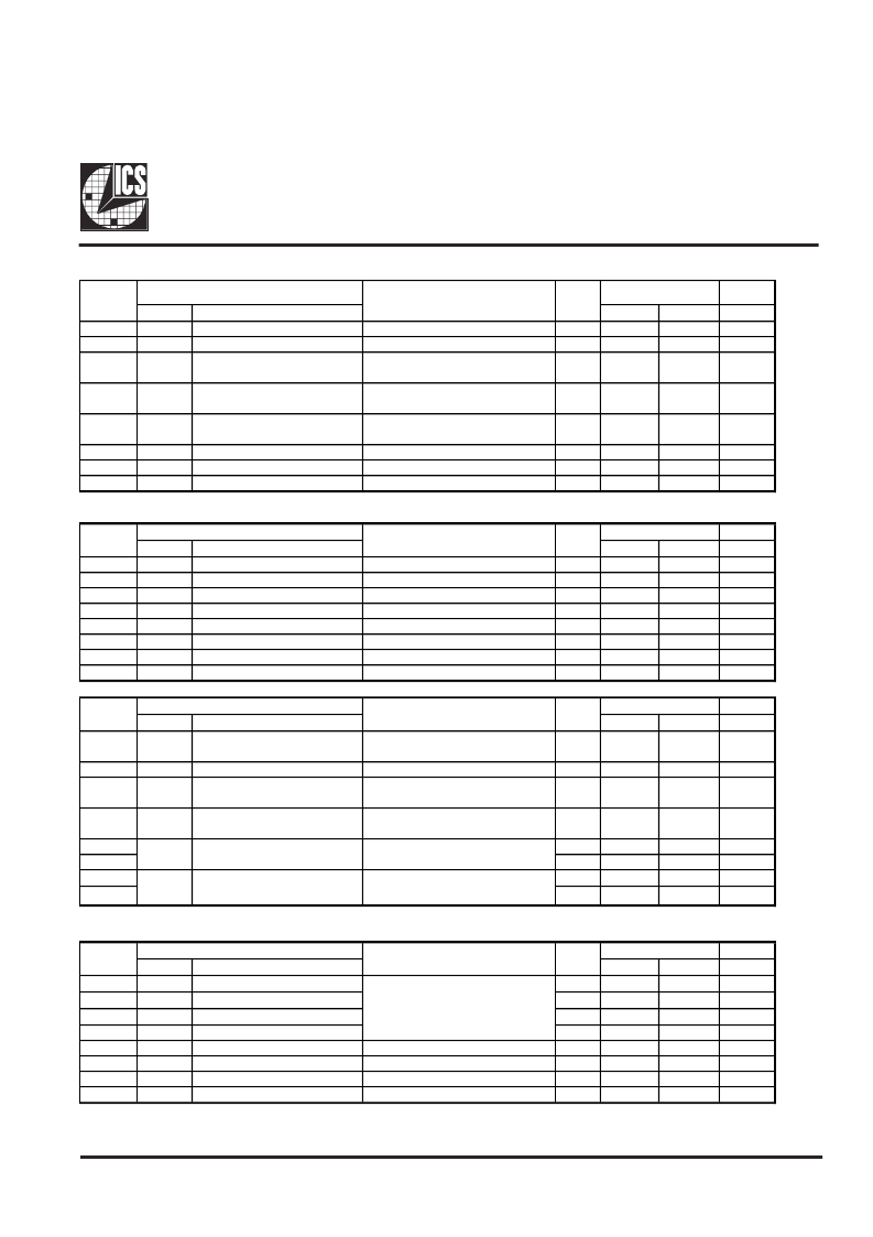
7
ICS950813
Advance Information
0708—10/10/02
Pin #
38
39
Name
0
1
PWD
1
1
Bit 7
Bit 6
48MHz_DOT
48MHz_USB/FS2**
Output control
Output control
Allow control of output with
assertion of PCI_STOP#.
Allow control of output with
assertion of PCI_STOP#.
Allow control of output with
assertion of PCI_STOP#.
Output control
Output control
Output control
RW
RW
Disable
Disable
Enable
Enable
Not
Freerun
Not
Freerun
Not
Freerun
Enable
Enable
Enable
Bit 5
7
*ASEL/PCICLK_F2 (see note)
RW
Freerun
0
Bit 4
6
PCICLK_F1 (see note)
RW
Freerun
0
Bit 3
5
PCICLK_F0 (see note)
RW
Freerun
0
Bit 2
Bit 1
Bit 0
Note:
7
6
5
*ASEL/PCICLK_F2
PCICLK_F1
PCICLK_F0
RW
RW
RW
Disable
Disable
Disable
1
1
1
Pin #
35
33
33
35
24
23
22
21
Name
FS3
FS4
0
-
-
1
-
-
PWD
X
X
1
1
1
1
1
1
Bit 7
Bit 6
Bit 5
Bit 4
Bit 3
Bit 2
Bit 1
Bit 0
Frequency Selection
Frequency Selection
Output control
Output control
Output control
Output control
Output control
Output control
RW
RW
RW
RW
RW
RW
RW
RW
3V66_0/FS4**
3V66_1/VCH_CLK/FS3**
3V66_5
3V66_4
3V66_3
3V66_2
Disable
Disable
Disable
Disable
Disable
Disable
Enable
Enable
Enable
Enable
Enable
Enable
Pin #
Name
0
1
PWD
Bit 7
X
PD Mode Iref Mirror Enable
Allow Iref Mirror to be ON during
Power Down Mode
Reserved
Allow control of output with
assertion of CPU_STOP#.
Allow control of output with
assertion of CPU_STOP#.
00 = Medium (default), 01 = Low,
11,10 =High
RW
OFF
ON
0
Bit 6
X
Reserved
X
-
-
0
Bit 5
X
3V66(5:2) (See table 6)
X
Freerun
Not
Freerun
Not
Freerun
-
-
-
-
0
Bit 4
X
3V66(1:0) (See table 7)
X
Freerun
0
Bit 3
Bit 2
Bit 1
Bit 0
Note:
RW
RW
RW
RW
-
-
-
-
0
0
0
0
Pin #
X
X
X
X
X
X
X
X
Name
0
-
-
-
-
-
-
-
-
1
-
-
-
-
-
-
-
-
PWD
0
0
0
0
0
0
0
1
Bit 7
Bit 6
Bit 5
Bit 4
Bit 3
Bit 2
Bit 1
Bit 0
Revision ID Bit 3
Revision ID Bit 2
Revision ID Bit 1
Revision ID Bit 0
Vendor ID Bit 3
Vendor ID Bit 2
Vendor ID Bit 1
Vendor ID Bit 0
R
R
R
R
R
R
R
R
(Reserved)
(Reserved)
(Reserved)
(Reserved)
Affected Pin
BYTE
6
Functions in Byte 5 of CK408 were intended as a test and debug byte only.
00 = Medium (default), 01 = Low,
11,10 =High
Bit Control
Bit Control
Type
39
48MHz_USB Slew Control
48MHz_DOT Slew Control
38
BYTE
4
Affected Pin
BYTE
5
Control Function
Affected Pin
Bit Control
Type
BYTE
3
PCICLK_F(2:0) can be turned on/off by PCI_STOP#. Refer to table 5.
Control Function
Control Function
Type
Bit Control
Type
Control Function
Affected Pin
Revision ID Value Based on
Device Revision
相關(guān)PDF資料 |
PDF描述 |
|---|---|
| ICS950818 | Frequency Generator with 200MHz Differential CPU Clocks |
| ICS950901 | Programmable Timing Control Hub for P4 |
| ICS950901YFLFT | TRIMMER, 500K |
| ICS950902YGLF-T | Programmable Timing Control Hub⑩ for P4⑩ |
| ICS950902 | Programmable Timing Control Hub⑩ for P4⑩ |
相關(guān)代理商/技術(shù)參數(shù) |
參數(shù)描述 |
|---|---|
| ICS950818 | 制造商:ICS 制造商全稱:ICS 功能描述:Frequency Generator with 200MHz Differential CPU Clocks |
| ICS950818YG-T | 制造商:ICS 制造商全稱:ICS 功能描述:Frequency Generator with 200MHz Differential CPU Clocks |
| ICS950901 | 制造商:ICS 制造商全稱:ICS 功能描述:Programmable Timing Control Hub for P4 |
| ICS950901YFLFT | 制造商:ICS 制造商全稱:ICS 功能描述:Programmable Timing Control Hub for P4 |
| ICS950902 | 制造商:ICS 制造商全稱:ICS 功能描述:Programmable Timing Control Hub⑩ for P4⑩ |
發(fā)布緊急采購,3分鐘左右您將得到回復(fù)。