- 您現(xiàn)在的位置:買賣IC網(wǎng) > PDF目錄360786 > ICS950813YGT Frequency Generator with 200MHz Differential CPU Clocks PDF資料下載
參數(shù)資料
| 型號(hào): | ICS950813YGT |
| 英文描述: | Frequency Generator with 200MHz Differential CPU Clocks |
| 中文描述: | 頻率發(fā)生器200MHz的CPU的時(shí)鐘差分 |
| 文件頁數(shù): | 11/22頁 |
| 文件大?。?/td> | 265K |
| 代理商: | ICS950813YGT |
11
ICS950813
Advance Information
0708—10/10/02
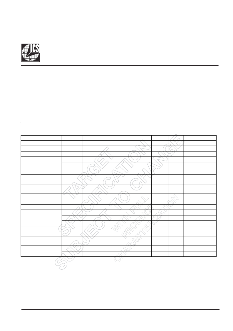
Absolute Maximum Ratings
Supply Voltage. . . . . . . . . . . . . . . . . . . . . . . . . 5.5 V
Logic Inputs . . . . . . . . . . . . . . . . . . . . . . . . . . . GND –0.5 V to V
DD
+ 0.5 V
Ambient Operating Temperature . . . . . . . . . . 0°C to +90°C
Case Temperature . . . . . . . . . . . . . . . . . . . . . . 115°C
Storage Temperature . . . . . . . . . . . . . . . . . . . . –65°C to +150°C
Stresses above those listed under
Absolute Maximum Ratings
may cause permanent damage to the device. These ratings
are stress specifications only and functional operation of the device at these or any other conditions above those listed
in the operational sections of the specifications is not implied. Exposure to absolute maximum rating conditions for
extended periods may affect product reliability.
Electrical Characteristics - Input/Supply/Common Output Parameters
T
A
= 0 - 70°C; Supply Voltage V
DD
= 3.3 V +/-5%
PARAMETER
SYMBOL
Input High Voltage
V
IH
Input Low Voltage
V
IL
Input High Current
I
IH
V
IN
= V
DD
I
IL1
V
IN
= 0 V; Inputs with no pull-up resistors
Input Low Current
CONDITIONS
MIN
2
TYP
MAX
UNITS
V
V
mA
mA
V
DD
+ 0.3
0.8
5
V
SS
- 0.3
-5
-5
I
IL2
V
IN
= 0 V; Inputs with pull-up resistors
-200
Operating Supply
Current
I
DD3.3OP
C
L
= Full load; Select @ 100 MHz
229
280
mA
I
DD3.3OP
C
L
=Full load; Select @ 133 MHz
IREF=5 mA
V
DD
= 3.3 V
220
280
45
mA
Powerdown Current
Input Frequency
Pin Inductance
I
DD3.3PD
F
i
L
pin
C
IN
C
OUT
C
INX
mA
MHz
nH
pF
pF
pF
7
5
6
Logic Inputs
Output pin capacitance
X1 & X2 pins
From Assertion of PWRSAVE# to 1st
clock.
From PowerUp or deassertion of
PowerDown to 1st clock.
Output enable delay (all outputs)
Output disable delay (all outputs)
27
30
33
PWRSAVE
Stabilization
1,2
T
PWRSV
1.8
ms
Clk Stabilization
1,2
T
STAB
1.8
ms
t
PZH
,t
PZL
t
PHZ
,t
PLZ
1
1
10
10
ns
ns
1
Guaranteed by design, not 100% tested in production.
2
See timing diagrams for buffered and un-buffered timing requirements.
Delay
1
Input Capacitance
1
相關(guān)PDF資料 |
PDF描述 |
|---|---|
| ICS950818 | Frequency Generator with 200MHz Differential CPU Clocks |
| ICS950901 | Programmable Timing Control Hub for P4 |
| ICS950901YFLFT | TRIMMER, 500K |
| ICS950902YGLF-T | Programmable Timing Control Hub⑩ for P4⑩ |
| ICS950902 | Programmable Timing Control Hub⑩ for P4⑩ |
相關(guān)代理商/技術(shù)參數(shù) |
參數(shù)描述 |
|---|---|
| ICS950818 | 制造商:ICS 制造商全稱:ICS 功能描述:Frequency Generator with 200MHz Differential CPU Clocks |
| ICS950818YG-T | 制造商:ICS 制造商全稱:ICS 功能描述:Frequency Generator with 200MHz Differential CPU Clocks |
| ICS950901 | 制造商:ICS 制造商全稱:ICS 功能描述:Programmable Timing Control Hub for P4 |
| ICS950901YFLFT | 制造商:ICS 制造商全稱:ICS 功能描述:Programmable Timing Control Hub for P4 |
| ICS950902 | 制造商:ICS 制造商全稱:ICS 功能描述:Programmable Timing Control Hub⑩ for P4⑩ |
發(fā)布緊急采購(gòu),3分鐘左右您將得到回復(fù)。