- 您現(xiàn)在的位置:買賣IC網(wǎng) > PDF目錄360779 > ICS9150-08 Frequency Generator & Integrated Buffers for Pentium/Pro⑩ PDF資料下載
參數(shù)資料
| 型號: | ICS9150-08 |
| 英文描述: | Frequency Generator & Integrated Buffers for Pentium/Pro⑩ |
| 中文描述: | 頻率發(fā)生器 |
| 文件頁數(shù): | 10/14頁 |
| 文件大小: | 329K |
| 代理商: | ICS9150-08 |
10
ICS9150-01
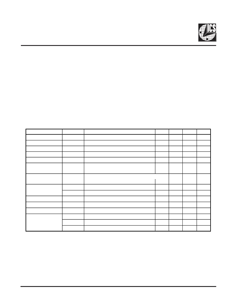
Absolute Maximum Ratings
Supply Voltage . . . . . . . . . . . . . . . . . . . . . . . . . . 7.0 V
Logic Inputs . . . . . . . . . . . . . . . . . . . . . . . . . . . . GND –0.5 V to V
DD
+0.5 V
Ambient Operating Temperature. . . . . . . . . . . . 0°C to +70°C
Storage Temperature . . . . . . . . . . . . . . . . . . . . . –65°C to +150°C
Stresses above those listed under
Absolute Maximum Ratings
may cause permanent damage to the device. These ratings are
stress specifications only and functional operation of the device at these or any other conditions above those listed in the
operational sections of the specifications is not implied. Exposure to absolute maximum rating conditions for extended
periods may affect product reliability.
Electrical Characteristics - Input/Supply/Common Output Parameters
T
A
= 0 - 70C; Supply Voltage V
DD
= V
DDL
= 3.3 V +/-5% (unless otherwise stated)
PARAMETER
SYMBOL
CONDITIONS
Input High Voltage
V
IH
Input Low Voltage
V
IL
Input High Current
I
IH
V
IN
= V
DD
Input Low Current
I
IL1
V
IN
= 0 V; Inputs with no pull-up resistors
Input Low Current
I
IL2
V
IN
= 0 V; Inputs with pull-up resistors
Operating
I
DD3.3OP
C
L
= 0 pF; Select @ 66M
Supply Current
Outputs Disabled
I
DD3.3OE
C
L
= 0 pF; With input address to Vdd or GND
Supply Current
Input Capacitance
1
C
IN
Logic Inputs
C
INX
X1 & X2 pins
Transition Time
1
T
trans
To 1st crossing of target Freq.
Settling Time
1
T
s
From 1st crossing to 1% target Freq.
Clk Stabilization
1
T
STAB
From V
DD
= 3.3 V to 1% target Freq.
T
CPU-SDRAM2
V
T
= 1.5 V
Skew
1
T
CPU-PCI2
V
T
= 1.5 V
T
REF-IOAPIC
V
T
= 1.5 V
MIN
2
V
SS
-0.3
TYP
MAX
V
DD
+0.3
0.8
5
UNITS
V
V
μ
A
μ
A
μ
A
mA
0.1
2.0
-100
75
-5
-200
95
18
25
mA
5
pF
pF
ms
ms
ms
ps
ns
ps
27
36
45
3
5
5
3
200
2
900
500
4
1
相關PDF資料 |
PDF描述 |
|---|---|
| ICS9155-23N28L | Low Cost 20-Pin Frequency Generator |
| ICS9155-01W24L | 5015 RR 3#8 PIN PLUG |
| ICS9155-01W28L | 5015 RR 3#8 PIN PLUG |
| ICS9155-01W32L | 5015 RR 4#8 SKT RECP |
| ICS9155-02W14L | Low Cost 20-Pin Frequency Generator |
相關代理商/技術參數(shù) |
參數(shù)描述 |
|---|---|
| ICS9150F-01 | 制造商:ICS 功能描述: |
| ICS9150F02 | 制造商:未知廠家 制造商全稱:未知廠家 功能描述:Peripheral IC |
| ICS9150F-02 | 制造商:ICS 制造商全稱:ICS 功能描述:Pentium Pro™ and SDRAM Frequency Generator |
| ICS9150F-04 | 制造商:ICS 制造商全稱:ICS 功能描述:Pentium Pro⑩ and SDRAM Frequency Generator |
| ICS9150F04T | 制造商:ICS 功能描述:New |
發(fā)布緊急采購,3分鐘左右您將得到回復。