- 您現(xiàn)在的位置:買(mǎi)賣(mài)IC網(wǎng) > PDF目錄360752 > ICS650-36 Networking & PCI Clock Source PDF資料下載
參數(shù)資料
| 型號(hào): | ICS650-36 |
| 英文描述: | Networking & PCI Clock Source |
| 中文描述: | 網(wǎng)絡(luò) |
| 文件頁(yè)數(shù): | 3/7頁(yè) |
| 文件大小: | 117K |
| 代理商: | ICS650-36 |
Networking & PCI Clock Source
MDS 650-36 D
3
Revision 030206
Integrated Circuit Systems
●
525 Race Street, San Jose, CA 95126
●
tel (408) 297-1201
●
www.icst.com
ICS650-36
External Components
Decoupling Capacitor
As with any high performance mixed-signal IC, the
ICS650-36 must be isolated from system power supply
noise to perform optimally.
A decoupling capacitor of 0.01μF must be connected
between each VDD and the PCB ground plane.
Series Termination Resistor
Clock output traces over one inch should use series
termination. To series terminate a 50
trace (a
commonly used trace impedance), place a 33
resistor
in series with the clock line, as close to the clock output
pin as possible. The nominal impedance of the clock
output is 20
.
Crystal Load Capacitors
The device crystal connections should include pads for
small capacitors from X1 to ground and from X2 to
ground. These capacitors are used to adjust the stray
capacitance of the board to match the nominally
required crystal load capacitance. Because load
capacitance can only be increased in this trimming
process, it is important to keep stray capacitance to a
minimum by using very short PCB traces (and no vias)
between the crystal and device. Crystal capacitors
must be connected from each of the pins X1 and X2 to
ground.
The value (in pF) of these crystal caps should equal
(C
L
-6 pF)*2. In this equation, C
L
= crystal load
capacitance in pF. Example: For a crystal with a 16 pF
load capacitance, each crystal capacitor would be 20
pF [(16-6) x 2 = 20].
PCB Layout Recommendations
Observed the following guidelines for optimum device
performance and lowest output phase noise:
1) The 0.01μF decoupling capacitors should be
mounted on the component side of the board as close
to the VDD pin as possible. No vias should be used
between the decoupling capacitors and VDD pins. The
PCB trace to VDD pins should be kept as short as
possible, as should the PCB trace to the ground via.
2) The external crystal should be mounted just next to
the device with short traces. The X1 and X2 traces
should not be routed next to each other with minimum
spaces, instead they should be separated and away
from other traces.
3) Place the 33
series termination resistor (if needed)
close to the clock output to minimize EMI.
4) An optimum layout is one with all components on the
same side of the board, minimizing vias through other
signal layers. Other signal traces should be routed
away from the ICS650-36. This includes signal traces
just underneath the device, or on layers adjacent to the
ground plane layer used by the device.
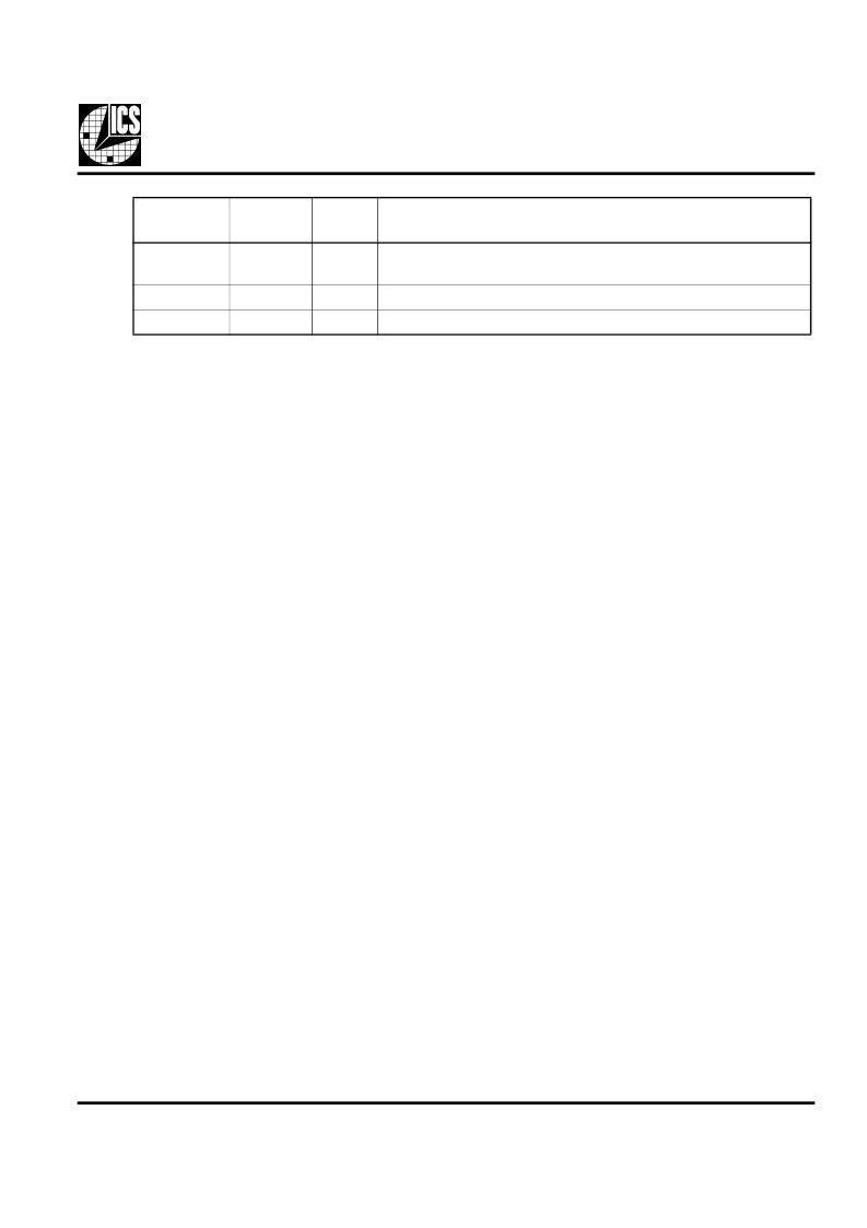
14
REF
Output
Reference 25 MHz clock output. Weak internal pull-down when
tri-state.
15
GND
Power
Connect to ground.
16
VDD
Power
Connect to +3.3 V.
Pin
Number
Pin
Name
Pin
Type
Pin Description
相關(guān)PDF資料 |
PDF描述 |
|---|---|
| ICS650G-36 | Networking & PCI Clock Source |
| ICS650G-36LF | Networking & PCI Clock Source |
| ICS650G-36LFT | Networking & PCI Clock Source |
| ICS650G-36T | Networking & PCI Clock Source |
| ICS650GI-36 | Networking & PCI Clock Source |
相關(guān)代理商/技術(shù)參數(shù) |
參數(shù)描述 |
|---|---|
| ICS650-40 | 制造商:ICS 制造商全稱(chēng):ICS 功能描述:ETHERNET SWITCH CLOCK SOURCE |
| ICS650-40A | 制造商:ICS 制造商全稱(chēng):ICS 功能描述:ETHERNET SWITCH CLOCK SOURCE |
| ICS650-41 | 制造商:ICS 制造商全稱(chēng):ICS 功能描述:Spread Spectrum Clock Synthesizer |
| ICS650-44 | 制造商:ICS 制造商全稱(chēng):ICS 功能描述:Spread Spectrum Clock Synthesizer |
| ICS650-47 | 制造商:ICS 制造商全稱(chēng):ICS 功能描述:Spread Spectrum Clock Synthesizer |
發(fā)布緊急采購(gòu),3分鐘左右您將得到回復(fù)。