- 您現(xiàn)在的位置:買賣IC網(wǎng) > PDF目錄61069 > ICS525RI-07 250 MHz, OTHER CLOCK GENERATOR, PDSO28 PDF資料下載
參數(shù)資料
| 型號: | ICS525RI-07 |
| 元件分類: | 時鐘產(chǎn)生/分配 |
| 英文描述: | 250 MHz, OTHER CLOCK GENERATOR, PDSO28 |
| 封裝: | 0.150 INCH, MO-153, SSOP-28 |
| 文件頁數(shù): | 1/9頁 |
| 文件大小: | 185K |
| 代理商: | ICS525RI-07 |
ICS525-07/08
MDS 525-07/08
B
1
Revision 031706
Integrated Circuit Systems, Inc.
● 525 Race Street, San Jose, CA 95126 ● tel (408) 297-1201 ● www.icst.com
LVCMOS User Configurable Clock
PRELIMINARY INFORMATION
Description
The ICS525-07/08 are the most flexible way to
generate a high-quality clock output from an
inexpensive crystal or clock input at low supply
voltages. The user can configure the device to produce
nearly any output frequency from any input frequency
by grounding or floating the select pins or by driving or
hard wiring the select pins high or low. Neither
microcontroller, software, nor device programmer are
needed to set the frequency. Using Phase-Locked
Loop (PLL) techniques, the device accepts a standard
fundamental mode, inexpensive crystal to produce
output clocks up to 250 MHz. It can also produce a
highly accurate output clock from a given input clock,
keeping them frequency locked.
For similar capability with a serial interface, use the
ICS307.
This product is intended for clock generation. It has low
output jitter (variation in the output period), but input to
output skew is not defined nor guaranteed.
Features
Packaged as 28-pin SSOP (150 mil body)
Available in Pb (lead) free package, RoHS 5/6
compliant
User determines the output frequency by setting all
internal dividers
Eliminates need for custom oscillators
Low voltage operation
Pull-ups on all select inputs
Input crystal frequency of 5 - 27 MHz
Input clock frequency of 2 - 50 MHz
Compensated loop bandwidth
Enhanced low frequency operation (-08 version)
Low jitter
Duty cycle of 45/55 up to 250 MHz
Operating voltage of 1.8 V to 2.5 V
Ideal for oscillator replacement
Available in commercial and industrial temperature
ranges
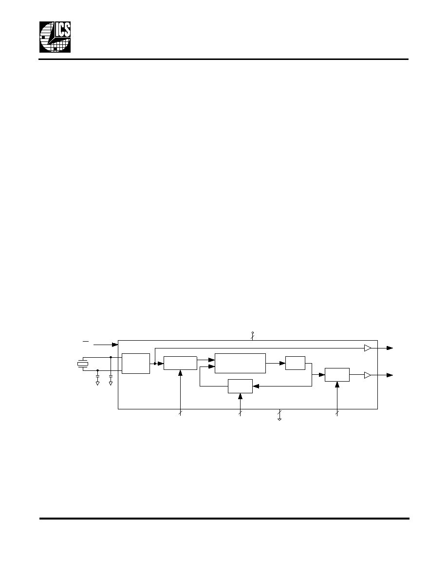
Block Diagram
VDD
GND
2
CLK
REF
Reference
Divider
Phase Comparator,
Charge Pump, and
Loop Filter
VCO
Divider
Output
Divider
R Configuration Pins
V Configuration Pins
S Configuration Pins
X1/ICLK
X2
Crystal or clock
input
Optional crystal capacitors
Crystal
Oscillator
PD
VDD
GND
2
CLK
REF
Reference
Divider
Phase Comparator,
Charge Pump, and
Loop Filter
VCO
Divider
Output
Divider
R Configuration Pins
V Configuration Pins
S Configuration Pins
X1/ICLK
X2
Crystal or clock
input
Optional crystal capacitors
Crystal
Oscillator
PD
相關(guān)PDF資料 |
PDF描述 |
|---|---|
| ICS525RI-07T | 250 MHz, OTHER CLOCK GENERATOR, PDSO28 |
| ICS527R-02LFT | 527 SERIES, PLL BASED CLOCK DRIVER, 2 TRUE OUTPUT(S), 0 INVERTED OUTPUT(S), PDSO28 |
| ICS527R-02LF | 527 SERIES, PLL BASED CLOCK DRIVER, 2 TRUE OUTPUT(S), 0 INVERTED OUTPUT(S), PDSO28 |
| ICS527R-02LF | 527 SERIES, PLL BASED CLOCK DRIVER, 2 TRUE OUTPUT(S), 0 INVERTED OUTPUT(S), PDSO28 |
| ICS527R-02IT | 527 SERIES, PLL BASED CLOCK DRIVER, 2 TRUE OUTPUT(S), 0 INVERTED OUTPUT(S), PDSO28 |
相關(guān)代理商/技術(shù)參數(shù) |
參數(shù)描述 |
|---|---|
| ICS525RI07LF | 制造商:ICS 制造商全稱:ICS 功能描述:LVCMOS User Configurable Clock |
| ICS525RI-07LF | 制造商:ICS 制造商全稱:ICS 功能描述:LVCMOS User Configurable Clock |
| ICS525RI-07LFT | 制造商:ICS 制造商全稱:ICS 功能描述:LVCMOS User Configurable Clock |
| ICS525RI-07T | 制造商:ICS 制造商全稱:ICS 功能描述:LVCMOS User Configurable Clock |
| ICS525RI-08 | 制造商:ICS 制造商全稱:ICS 功能描述:LVCMOS User Configurable Clock |
發(fā)布緊急采購,3分鐘左右您將得到回復(fù)。