- 您現(xiàn)在的位置:買賣IC網(wǎng) > PDF目錄360716 > IC42S16100-7TIG 512K x 16 Bits x 2 Banks (16-MBIT) SYNCHRONOUS DYNAMIC RAM PDF資料下載
參數(shù)資料
| 型號(hào): | IC42S16100-7TIG |
| 英文描述: | 512K x 16 Bits x 2 Banks (16-MBIT) SYNCHRONOUS DYNAMIC RAM |
| 中文描述: | 為512k × 16位× 2組(16兆)同步動(dòng)態(tài)RAM |
| 文件頁數(shù): | 2/78頁 |
| 文件大?。?/td> | 789K |
| 代理商: | IC42S16100-7TIG |
第1頁當(dāng)前第2頁第3頁第4頁第5頁第6頁第7頁第8頁第9頁第10頁第11頁第12頁第13頁第14頁第15頁第16頁第17頁第18頁第19頁第20頁第21頁第22頁第23頁第24頁第25頁第26頁第27頁第28頁第29頁第30頁第31頁第32頁第33頁第34頁第35頁第36頁第37頁第38頁第39頁第40頁第41頁第42頁第43頁第44頁第45頁第46頁第47頁第48頁第49頁第50頁第51頁第52頁第53頁第54頁第55頁第56頁第57頁第58頁第59頁第60頁第61頁第62頁第63頁第64頁第65頁第66頁第67頁第68頁第69頁第70頁第71頁第72頁第73頁第74頁第75頁第76頁第77頁第78頁
IC42S16100
2
Integrated Circuit Solution Inc.
DR024-0D 06/25/2004
ICSI reserves the right to make changes to its products at any time without notice in order to improve design and supply the best possible product. We assume no responsibility for any errors
which may appear in this publication. Copyright 2000, Integrated Circuit Solution Inc.
FEATURES
Clock frequency: 200, 166, 143 MHz
Fully synchronous; all signals referenced to a
positive clock edge
Two banks can be operated simultaneously and
independently
Dual internal bank controlled by A11 (bank select)
Single 3.3V power supply
LVTTL interface
Programmable burst length
– (1, 2, 4, 8, full page)
Programmable burst sequence:
Sequential/Interleave
Auto refresh, self refresh
4096 refresh cycles every 64 ms
Random column address every clock cycle
Programmable
CAS
latency (2, 3 clocks)
Burst read/write and burst read/single write
operations capability
Burst termination by burst stop and precharge
command
Byte controlled by LDQM and UDQM
Package 400mil 50-pin TSOP-2
Pb(lead)-free package is available
DESCRIPTION
ICSI
's 16Mb Synchronous DRAM IC42S16100 is organized
as a 524,288-word x 16-bit x 2-bank for improved
performance. The synchronous DRAMs achieve high-speed
data transfer using pipeline architecture. All inputs and
outputs signals refer to the rising edge of the clock input.
512K x 16 Bits x 2 Banks (16-MBIT)
SYNCHRONOUS DYNAMIC RAM
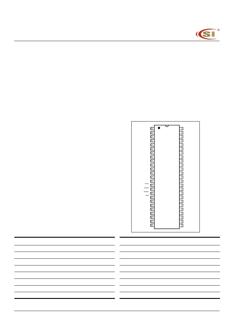
PIN CONFIGURATIONS
50-Pin TSOP-2
1
2
3
4
5
6
7
8
9
10
11
12
13
14
15
16
17
18
19
20
21
22
23
24
25
50
49
48
47
46
45
44
43
42
41
40
39
38
37
36
35
34
33
32
31
30
29
28
27
26
VCC
I/O0
I/O1
GNDQ
I/O2
I/O3
VCCQ
I/O4
I/O5
GNDQ
I/O6
I/O7
VCCQ
LDQM
WE
CAS
RAS
CS
A11
A10
A0
A1
A2
A3
VCC
GND
I/O15
I/O14
GNDQ
I/O13
I/O12
VCCQ
I/O11
I/O10
GNDQ
I/O9
I/O8
VCCQ
NC
UDQM
CLK
CKE
NC
A9
A8
A7
A6
A5
A4
GND
PIN DESCRIPTIONS
A0-A11
Address Input
A0-A10
Row Address Input
A11
Bank Select Address
A0-A7
Column Address Input
I/O0 to I/O15
Data I/O
CLK
System Clock Input
CKE
Clock Enable
CS
Chip Select
RAS
Row Address Strobe Command
CAS
Column Address Strobe Command
WE
Write Enable
LDQM
Lower Bye, Input/Output Mask
UDQM
Upper Bye, Input/Output Mask
Vcc
Power
GND
Ground
VccQ
Power Supply for I/O Pin
GNDQ
Ground for I/O Pin
NC
No Connection
相關(guān)PDF資料 |
PDF描述 |
|---|---|
| IC42S16400-7TIG | 1M x 16Bit x 4 Banks (64-MBIT) SDRAM |
| IC42S16400 | 1M x 16Bit x 4 Banks (64-MBIT) SDRAM |
| IC42S16400-6BG | RES 100-OHM 5% 0.1W 200PPM THICK-FILM SMD-0603 5K/REEL-7IN-PA |
| IC42S16400-6BIG | 1M x 16Bit x 4 Banks (64-MBIT) SDRAM |
| IC42S16400-6T | 1M x 16Bit x 4 Banks (64-MBIT) SDRAM |
相關(guān)代理商/技術(shù)參數(shù) |
參數(shù)描述 |
|---|---|
| IC42S16101 | 制造商:ICSI 制造商全稱:Integrated Circuit Solution Inc 功能描述:512K x 16 Bit x 2 Banks (16-MBIT) SDRAM |
| IC42S16101-5BG | 制造商:ICSI 制造商全稱:Integrated Circuit Solution Inc 功能描述:512K x 16 Bit x 2 Banks (16-MBIT) SDRAM |
| IC42S16101-5BIG | 制造商:ICSI 制造商全稱:Integrated Circuit Solution Inc 功能描述:512K x 16 Bit x 2 Banks (16-MBIT) SDRAM |
| IC42S16101-5T | 制造商:ICSI 制造商全稱:Integrated Circuit Solution Inc 功能描述:512K x 16 Bit x 2 Banks (16-MBIT) SDRAM |
| IC42S16101-5TG | 制造商:ICSI 制造商全稱:Integrated Circuit Solution Inc 功能描述:512K x 16 Bit x 2 Banks (16-MBIT) SDRAM |
發(fā)布緊急采購,3分鐘左右您將得到回復(fù)。