- 您現(xiàn)在的位置:買賣IC網(wǎng) > PDF目錄224000 > HYS72T64000EP-3.7-B2 (QIMONDA AG) 64M X 72 DDR DRAM MODULE, DMA240 PDF資料下載
參數(shù)資料
| 型號(hào): | HYS72T64000EP-3.7-B2 |
| 廠商: | QIMONDA AG |
| 元件分類: | DRAM |
| 英文描述: | 64M X 72 DDR DRAM MODULE, DMA240 |
| 封裝: | GREEN, RDIMM-240 |
| 文件頁數(shù): | 10/64頁 |
| 文件大小: | 3411K |
| 代理商: | HYS72T64000EP-3.7-B2 |
第1頁第2頁第3頁第4頁第5頁第6頁第7頁第8頁第9頁當(dāng)前第10頁第11頁第12頁第13頁第14頁第15頁第16頁第17頁第18頁第19頁第20頁第21頁第22頁第23頁第24頁第25頁第26頁第27頁第28頁第29頁第30頁第31頁第32頁第33頁第34頁第35頁第36頁第37頁第38頁第39頁第40頁第41頁第42頁第43頁第44頁第45頁第46頁第47頁第48頁第49頁第50頁第51頁第52頁第53頁第54頁第55頁第56頁第57頁第58頁第59頁第60頁第61頁第62頁第63頁第64頁
HYS72T[64/128/256]xx0EP–[2.5/25F/3/3S/3.7]–B2
Registered DDR2 SDRAM Modules
Internet Data Sheet
Rev. 1.02, 2008-06
18
07312007-HYD2-P177
2) The CK/CK input reference level (for timing reference to CK/CK) is the point at which CK and CK cross. The DQS / DQS, RDQS / RDQS,
input reference level is the crosspoint when in differential strobe mode.
3) Inputs are not recognized as valid until
V
REF stabilizes. During the period before VREF stabilizes, CKE = 0.2 x VDDQ
4) The output timing reference voltage level is
V
TT.
5)
t
RAS.MAX is calculated from the maximum amount of time a DDR2 device can operate without a refresh command which is equal to 9 x tREFI.
6) Products released after 2007-08-01 can support
t
RAS.MIN = 40 ns for all DDR2 speed sort.
7) For products released after 2007-08-01.
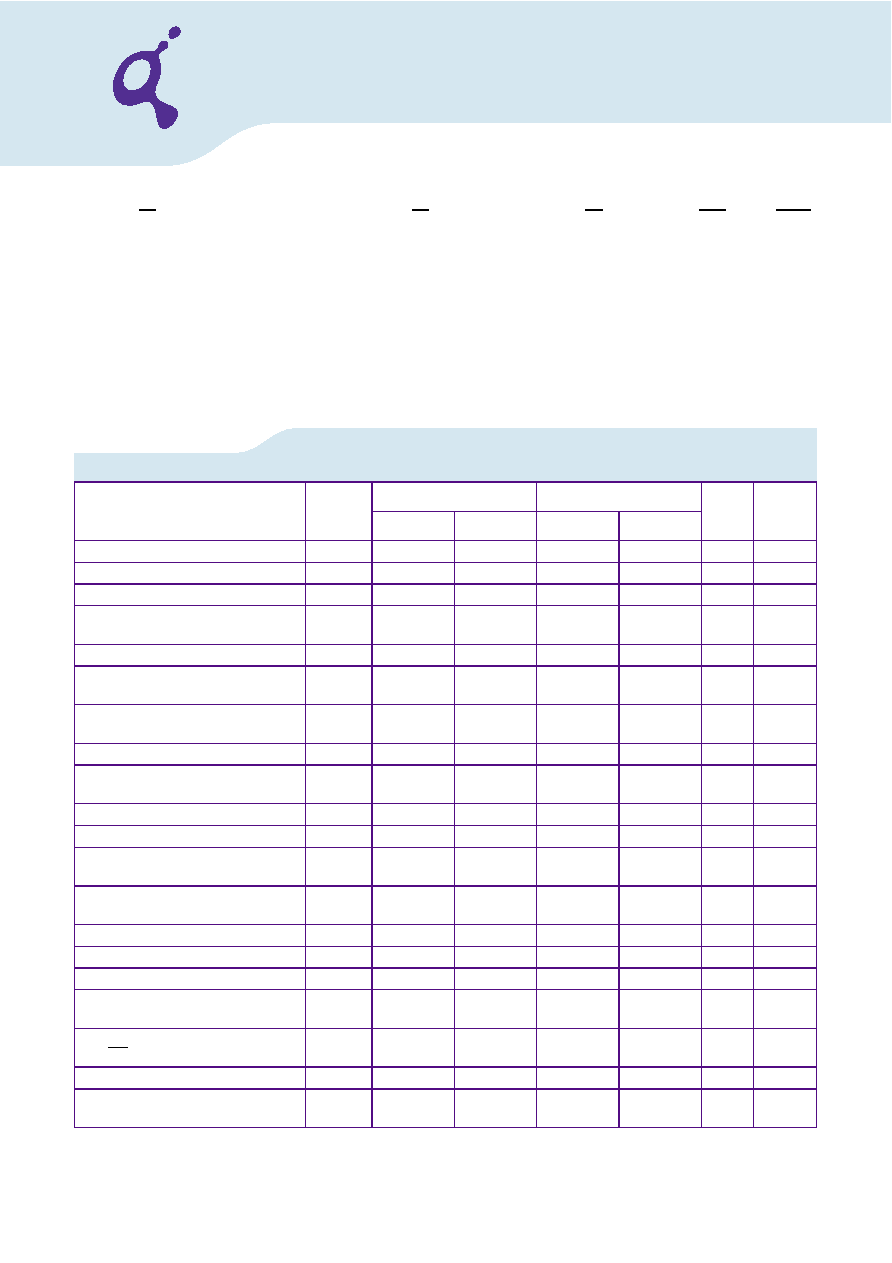
3.4
Component AC Timing Parameters
TABLE 14
DRAM Component Timing Parameter by Speed Grade - DDR2–800 and DDR2–667
Parameter
Symbol
DDR2–800
DDR2–667
Unit
Min.
Max.
Min.
Max.
CAS to CAS command delay
t
CCD
2—
nCK
Average clock high pulse width
t
CH.AVG
0.48
0.52
0.48
0.52
t
CK.AVG
Average clock period
t
CK.AVG
2500
8000
3000
8000
ps
CKE minimum pulse width ( high and
low pulse width)
t
CKE
3—
nCK
Average clock low pulse width
t
CL.AVG
0.48
0.52
0.48
0.52
t
CK.AVG
Auto-Precharge write recovery +
precharge time
t
DAL
WR +
t
nRP
—WR +
t
nRP
—nCK
Minimum time clocks remain ON after
CKE asynchronously drops LOW
t
DELAY
t
IS + tCK .AVG
+
t
IH
––
t
IS +
t
CK .AVG + tIH
––
ns
DQ and DM input hold time
t
DH.BASE
125
––
175
––
ps
DQ and DM input pulse width for each
input
t
DIPW
0.35
—
0.35
—
t
CK.AVG
DQS input high pulse width
t
DQSH
0.35
—
0.35
—
t
CK.AVG
DQS input low pulse width
t
DQSL
0.35
—
0.35
—
t
CK.AVG
DQS-DQ skew for DQS & associated
DQ signals
t
DQSQ
—
200
—
240
ps
DQS latching rising transition to
associated clock edges
t
DQSS
– 0.25
+ 0.25
– 0.25
+ 0.25
t
CK.AVG
DQ and DM input setup time
t
DS.BASE
50
––
100
––
ps
DQS falling edge hold time from CK
t
DSH
0.2
—
0.2
—
t
CK.AVG
DQS falling edge to CK setup time
t
DSS
0.2
—
0.2
—
t
CK.AVG
CK half pulse width
t
HP
Min(
t
CH.ABS,
t
CL.ABS)
__
Min(
t
CH.ABS,
t
CL.ABS)
__
ps
Data-out high-impedance time from
CK / CK
t
HZ
—
t
AC.MAX
—
t
AC.MAX
ps
Address and control input hold time
t
IH.BASE
250
—
275
—
ps
Control & address input pulse width
for each input
t
IPW
0.6
—
0.6
—
t
CK.AVG
相關(guān)PDF資料 |
PDF描述 |
|---|---|
| HZ20-1 | 19.25 V, 0.5 W, SILICON, UNIDIRECTIONAL VOLTAGE REGULATOR DIODE, DO-35 |
| HZ6B1L | 5.65 V, 0.4 W, SILICON, UNIDIRECTIONAL VOLTAGE REGULATOR DIODE, DO-35 |
| HZ9.1CP | 9.65 V, 1 W, SILICON, UNIDIRECTIONAL VOLTAGE REGULATOR DIODE, DO-41 |
| HZB6.8MWA | 6.8 V, 0.2 W, SILICON, UNIDIRECTIONAL VOLTAGE REGULATOR DIODE |
| HZF24BPTR | 0.9 W, SILICON, UNIDIRECTIONAL VOLTAGE REGULATOR DIODE |
相關(guān)代理商/技術(shù)參數(shù) |
參數(shù)描述 |
|---|---|
| HYS72T64000EU-2.5-B2 | 制造商:QIMONDA 制造商全稱:QIMONDA 功能描述:240-Pin unbuffered DDR2 SDRAM Modules |
| HYS72T64000EU-25F-B2 | 制造商:QIMONDA 制造商全稱:QIMONDA 功能描述:240-Pin unbuffered DDR2 SDRAM Modules |
| HYS72T64000EU-3.7-B2 | 制造商:QIMONDA 制造商全稱:QIMONDA 功能描述:240-Pin unbuffered DDR2 SDRAM Modules |
| HYS72T64000EU-3-B2 | 制造商:QIMONDA 制造商全稱:QIMONDA 功能描述:240-Pin unbuffered DDR2 SDRAM Modules |
| HYS72T64000EU-3S-B2 | 制造商:QIMONDA 制造商全稱:QIMONDA 功能描述:240-Pin unbuffered DDR2 SDRAM Modules |
發(fā)布緊急采購(gòu),3分鐘左右您將得到回復(fù)。