- 您現(xiàn)在的位置:買賣IC網(wǎng) > PDF目錄224000 > HYMD264G726A4-H (HYNIX SEMICONDUCTOR INC) 64M X 72 DDR DRAM MODULE, 0.75 ns, DMA184 PDF資料下載
參數(shù)資料
| 型號: | HYMD264G726A4-H |
| 廠商: | HYNIX SEMICONDUCTOR INC |
| 元件分類: | DRAM |
| 英文描述: | 64M X 72 DDR DRAM MODULE, 0.75 ns, DMA184 |
| 封裝: | 5.250 X 1.700 X 0.150 INCH, DIMM-184 |
| 文件頁數(shù): | 7/16頁 |
| 文件大小: | 257K |
| 代理商: | HYMD264G726A4-H |
HYMD264G726A(L)4-M/K/H/L
Rev. 0.2/May. 02
15
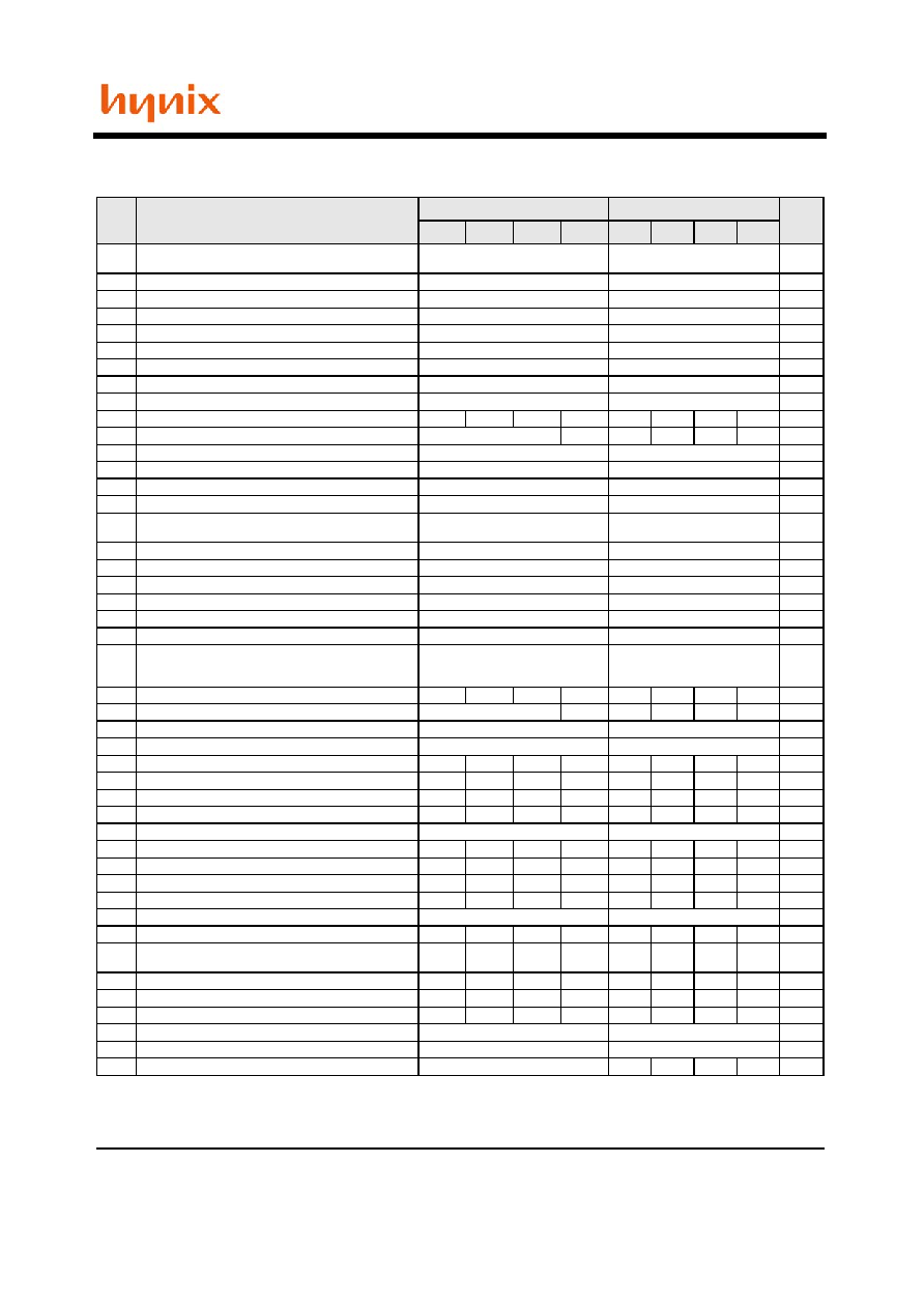
SERIAL PRESENCE DETECT
Byte#
Function Description
Function Supported
Hexa Value
Note
M
K
H
L
M
K
H
L
0
Number of Bytes written into serial memory at module
manufacturer
128 Bytes
80h
1
Total number of Bytes in SPD device
256 Bytes
08h
2
Fundamental memory type
DDR SDRAM
07h
3
Number of row address on this assembly
13
0Dh
1
4
Number of column address on this assembly
11
0Bh
1
5
Number of physical banks on DIMM
1Bank
01h
6
Module data width
72 Bits
48h
7
Module data width (continued)
-
00h
8
Module voltage Interface levels(VDDQ)
SSTL 2.5V
04h
9
DDR SDRAM cycle time at CAS Latency=2.5(tCK)
7.5ns
8.0ns
75h
80h
2
10
DDR SDRAM access time from clock at CL=2.5 (tAC)
+/-0.75ns
+/-0.8ns
75h
80h
2
11
Module configuration type
ECC
02h
12
Refresh rate and type
7.8us & Self refresh
82h
13
Primary DDR SDRAM width
x4
04h
14
Error checking DDR SDRAM data width
x4
04h
15
Minimum clock delay for back-to-back random column
address(tCCD)
1 CLK
01h
16
Burst lengths supported
2,4,8
0Eh
17
Number of banks on each DDR SDRAM
4 Banks
04h
18
CAS latency supported
2, 2.5
0Ch
19
CS latency
0
01h
20
WE latency
1
02h
21
DDR SDRAM module attributes
Registered, PLL
26h
22
DDR SDRAM device attributes : General
+/-0.2Voltage tolerance,
Concurrent Auto Precharge
tRAS Lock Out
C0h
23
DDR SDRAM cycle time at CL=2.0(tCK)
7.5ns
10ns
75h
A0h
2
24
DDR SDRAM access time from clock at CL=2.0(tAC)
+/-0.75ns
+/-0.8ns
75h
80h
2
25
DDR SDRAM cycle time at CL=1.5(tCK)
-
00h
2
26
DDR SDRAM access time from clock at CL=1.5(tAC)
-
00h
2
27
Minimum row precharge time(tRP)
15ns
20ns
3Ch
50h
28
Minimum row activate to row active delay(tRRD)
15ns
3Ch
29
Minimum RAS to CAS delay(tRCD)
15ns
20ns
3Ch
50h
30
Minimum active to precharge time(tRAS)
45ns
50ns
2Dh
32h
31
Module row density
512MB
80h
32
Command and address signal input setup time(tIS)
0.9ns
1.1ns
90h
B0h
33
Command and address signal input hold time(tIH)
0.9ns
1.1ns
90h
B0h
34
Data signal input setup time(tDS)
0.5ns
0.6ns
50h
60h
35
Data signal input hold time(tDH)
0.5ns
0.6ns
50h
60h
36~40 Reserved for VCSDRAM
Undefined
00h
41
Minimum active / auto-refresh time ( tRC)
60ns
65ns
70ns
3Ch
41h
46h
42
Minimum auto-refresh to active/auto-refresh
command period(tRFC)
75ns
80ns
4Bh
50h
43
Maximum cycle time (tCK max)
12ns
30h
44
Maximim DQS-DQ skew time(tDQSQ)
0.5ns
0.6ns
32h
3Ch
45
Maximum read data hold skew factor(tQHS)
0.75ns
75h
46~61 Superset information(may be used in future)
Undefined
00h
62
SPD Revision code
Initial release
00h
63
Checksum for Bytes 0~62
-
DBh
08h
33h
CDh
Bin Sort :M(DDR266(2-2-2),K(DDR266A@CL=2)
H(DDR266B@CL=2.5),L(DDR200@CL=2)
相關(guān)PDF資料 |
PDF描述 |
|---|---|
| HYR164830G-653 | 48M X 16 RAMBUS MODULE, DMA84 |
| HYS64T16000HDL-2.5-A | 16M X 64 DDR DRAM MODULE, 0.4 ns, DMA200 |
| HYS72D64020GR-7-X | 64M X 72 DDR DRAM MODULE, 0.75 ns, DMA184 |
| HYS72D64020GR-7.5-X | 64M X 72 DDR DRAM MODULE, 0.75 ns, DMA184 |
| HYS72T128000EU-2.5-C2 | 128M X 72 DDR DRAM MODULE, 0.4 ns, DMA240 |
相關(guān)代理商/技術(shù)參數(shù) |
參數(shù)描述 |
|---|---|
| HYMD264G726A4-K | 制造商:HYNIX 制造商全稱:Hynix Semiconductor 功能描述:Registered DDR SDRAM DIMM |
| HYMD264G726A4-L | 制造商:HYNIX 制造商全稱:Hynix Semiconductor 功能描述:Registered DDR SDRAM DIMM |
| HYMD264G726A4M | 制造商:未知廠家 制造商全稱:未知廠家 功能描述:64Mx72|2.5V|M/K/H/L|x18|DDR SDRAM - Low Profile Registered DIMM 512MB |
| HYMD264G726A4-M | 制造商:HYNIX 制造商全稱:Hynix Semiconductor 功能描述:Registered DDR SDRAM DIMM |
| HYMD264G726A4M-H | 制造商:HYNIX 制造商全稱:Hynix Semiconductor 功能描述:Low Profile Registered DDR SDRAM DIMM |
發(fā)布緊急采購,3分鐘左右您將得到回復(fù)。