- 您現(xiàn)在的位置:買賣IC網(wǎng) > PDF目錄385400 > HT48R50A (Holtek Semiconductor Inc.) 8-BIT MICROCONTROLLER PDF資料下載
參數(shù)資料
| 型號(hào): | HT48R50A |
| 廠商: | Holtek Semiconductor Inc. |
| 元件分類: | 數(shù)學(xué)處理器 |
| 英文描述: | 8-BIT MICROCONTROLLER |
| 中文描述: | 8位微控制器 |
| 文件頁數(shù): | 4/46頁 |
| 文件大小: | 1037K |
| 代理商: | HT48R50A |
第1頁第2頁第3頁當(dāng)前第4頁第5頁第6頁第7頁第8頁第9頁第10頁第11頁第12頁第13頁第14頁第15頁第16頁第17頁第18頁第19頁第20頁第21頁第22頁第23頁第24頁第25頁第26頁第27頁第28頁第29頁第30頁第31頁第32頁第33頁第34頁第35頁第36頁第37頁第38頁第39頁第40頁第41頁第42頁第43頁第44頁第45頁第46頁
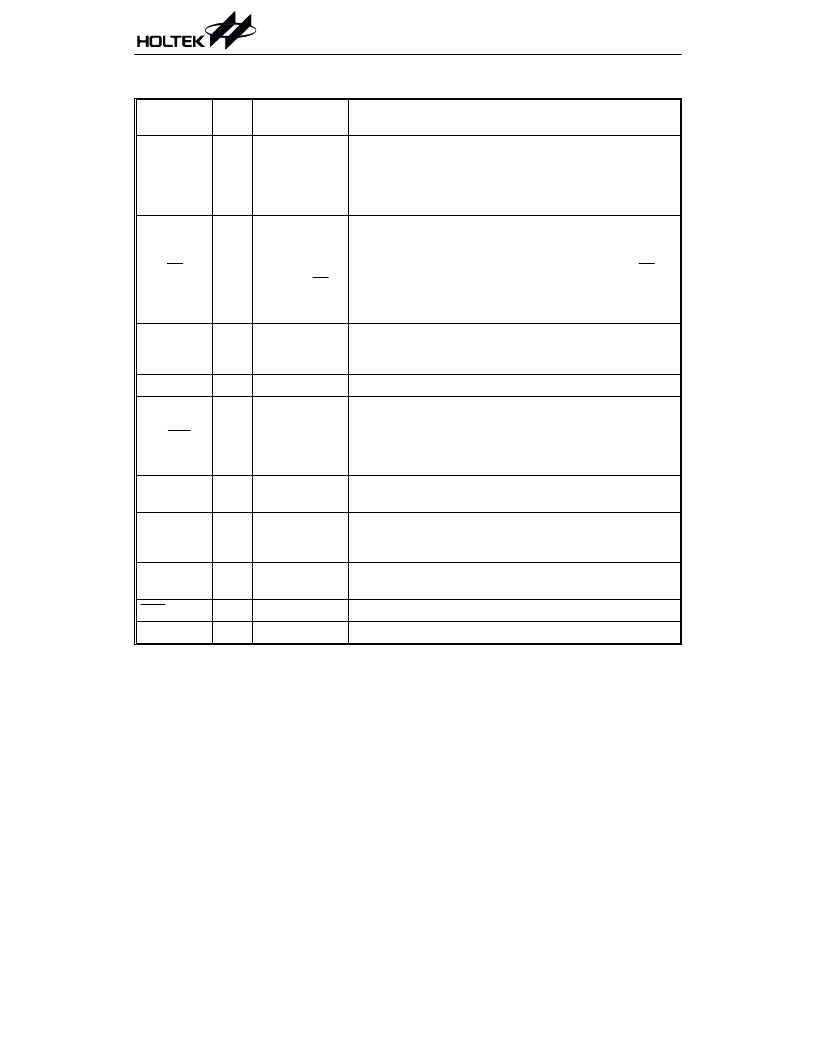
Pin Description
Pin Name
I/O
ROM Code
Option
Description
PA0~PA7
I/O
Pull-high*
Wake-up
CMOS/Schmitt
trigger input
Bidirectional 8-bit input/output port. Each bit can be con-
figured as a wake-up input by ROM code option. Software
instructions determine the CMOS output or Schmitt trigger
or CMOS input (depends on options) with pull-high resistor
(determined by 1-bit pull-high option).
PB0/BZ
PB1/BZ
PB2~PB7
I/O
Pull-high*
PB0 or BZ
PB1 or BZ
Bidirectional 8-bit input/output port. Software instructions
determine the CMOS output or Schmitt trigger input with
pull-high resistor (determined by 1-bit pull-high option).
The PB0 and PB1 are pin-shared with the BZ and BZ, re-
spectively. Once the PB0 or PB1 is selected as buzzer out-
put, the output signals come from an internal PFD
generator (shared with Timer/Event Counter 0).
PD0~PD7
I/O
Pull-high*
Bidirectional I/O lines. Software instructions determine the
CMOS output or Schmitt trigger input with pull-high resis-
tor (determined by 1-bit pull-high option).
VSS
Negative power supply, ground
PG0/INT
I/O
Pull-high*
Bidirectional I/O lines. Software instructions determine the
CMOS output or Schmitt trigger input with pull-high resis-
tor (determined by 1-bit pull-high option). This external in-
terrupt input is pin-shared with PG0. The external
interrupt input is activated on a high to low transition.
TMR0
I
Timer/Event Counter 0 Schmitt trigger input (without
pull-high resistor)
PC0~PC7
I/O
Pull-high*
Bidirectional I/O lines. Software instructions determine the
CMOS output or Schmitt trigger input with pull-high resis-
tor (determined by 1-bit pull-high option).
TMR1
I
Timer/Event Counter 1 Schmitt trigger input (without
pull-high resistor)
RES
I
Schmitt trigger reset input. Active low
VDD
Positive power supply
HT48R50A-1
Rev. 1.10
4
July 2, 2001
相關(guān)PDF資料 |
PDF描述 |
|---|---|
| HT48RA0A | 8-Bit Remote Type MCU |
| HT48RA3 | 8-Bit Remote Type OTP MCU |
| HT48RB8 | 8-Bit USB Type OTP MCU |
| HT49C10 | 8-BIT MICROCONTROLLER |
| HT49C30L | HDSP-A101 RED DISPLAY, LED, |
相關(guān)代理商/技術(shù)參數(shù) |
參數(shù)描述 |
|---|---|
| HT48R50A-1 | 制造商:HOLTEK 制造商全稱:Holtek Semiconductor Inc 功能描述:I/O Type 8-Bit MCU |
| HT48R50A-1_09 | 制造商:HOLTEK 制造商全稱:Holtek Semiconductor Inc 功能描述:I/O Type 8-Bit MCU |
| HT48R51 | 制造商:HOLTEK 制造商全稱:Holtek Semiconductor Inc 功能描述:8-Bit Microcontroller Series |
| HT48R51-1(28SKDIP-H0) | 制造商:未知廠家 制造商全稱:未知廠家 功能描述:8-Bit Microcontroller |
| HT48R51-1(40DIP-A0) | 制造商:未知廠家 制造商全稱:未知廠家 功能描述:8-Bit Microcontroller |
發(fā)布緊急采購,3分鐘左右您將得到回復(fù)。