- 您現(xiàn)在的位置:買賣IC網(wǎng) > PDF目錄67680 > HMC610LP4 (HITTITE MICROWAVE CORP) 0 MHz - 3900 MHz RF/MICROWAVE LINEAR DETECTOR, 20 dBm INPUT POWER-MAX PDF資料下載
參數(shù)資料
| 型號: | HMC610LP4 |
| 廠商: | HITTITE MICROWAVE CORP |
| 元件分類: | 檢測器 |
| 英文描述: | 0 MHz - 3900 MHz RF/MICROWAVE LINEAR DETECTOR, 20 dBm INPUT POWER-MAX |
| 封裝: | 4 X 4 MM, LEADLESS, PLASTIC, SMT, QFN-24 |
| 文件頁數(shù): | 11/22頁 |
| 文件大?。?/td> | 786K |
| 代理商: | HMC610LP4 |
For price, delivery, and to place orders, please contact Hittite Microwave Corporation:
20 Alpha Road, Chelmsford, MA 01824 Phone: 978-250-3343 Fax: 978-250-3373
Order On-line at www.hittite.com
P
O
W
E
R
D
E
T
E
C
T
O
R
S
-
SM
T
12
12 - 44
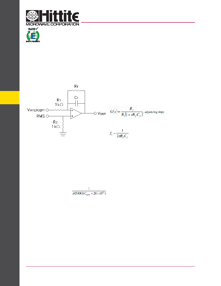
Log-Slope and Intercept
The HMC610LP4 is set with a Pin –> RMS transfer characteristic slope set to 36.5mV/dBm by design (otherwise
referred to as the log-slope). Connect the RMS pin directly to VSET pin. The Pin –> RMS transfer characteristic is
not adjustable internally, but both slope and intercept can be adjusted quite easily by using an external integrating
amplifier such as the one shown below. Avoid loading the RMS output with a capacitive load above 35pF, when
CINT<100pF.
Figure: External Integrating Amplifier with log-slope and log-intercept control.
VINTERCEPT is a DC voltage used to adjust the log-
intercept point.
VOUT(s)= RMSOUT X (1 + G(s)) - VINTERCEPT X G(s), V
, Hz = cut-off frequency
Rf is in Ohms
Cf is in Farads
DC Offset Compensation Loop
Internal DC offsets, which are input signal dependant, require continuous cancellation. Offset cancellation is a critical
function needed for maintenance of measurement accuracy and sensitivity. The DC offset cancellation loop performs
this function, and its response is largely defined by the capacitance off the COFS pin. Setting DC offset cancellation,
loop bandwidth strives to strike a balance between offset cancellation accuracy, and loop response time. A larger
value of COFS results in a more precise offset cancellation, but at the expense of a slower offset cancellation response.
A smaller value of COFS tilts the performance trade-off towards a faster offset cancellation response. The optimal loop
bandwidth setting will allow internal offsets to be cancelled at a minimally acceptable speed.
DC Offset Cancellation Loop ≈
Bandwidth , Hz
For example: loop bandwidth for DC cancellation with COFS = 1nF, bandwidth is ~62 kHz
Note:
The measurement error produced by internal DC offsets cannot be measured at any single operating point, in terms
of input signal frequency and level, with repeatability. Measurement error must be calculated to a best fit line, over the
entire operating range (again, in terms of signal level and frequency).
HMC610LP4 / 610LP4E
v12.0309
RMS POWER DETECTOR
75 dB, DC - 3.9 GHz
Standby Mode
The ENX can be used to force the power detector into a low-power standby mode. In this mode, the entire power
detector is powered-down. As ENX is deactivated, power is restored to all of the circuits. There is no memory of
previous conditions. Coming-out of stand-by, CINT and COFS capacitors will require recharging, so if large capacitor
values have been chosen, the wake-up time will be lengthened.
相關(guān)PDF資料 |
PDF描述 |
|---|---|
| HMC611 | 1 MHz - 10000 MHz RF/MICROWAVE THRESHOLD DETECTOR, 15 dBm INPUT POWER-MAX |
| HMC618LP3E | 1200 MHz - 2200 MHz RF/MICROWAVE NARROW BAND LOW POWER AMPLIFIER |
| HMC618LP3 | 1200 MHz - 2200 MHz RF/MICROWAVE NARROW BAND LOW POWER AMPLIFIER |
| HMC628LP4E | 50 MHz - 800 MHz RF/MICROWAVE WIDE BAND LOW POWER AMPLIFIER |
| HMC628LP4 | 50 MHz - 800 MHz RF/MICROWAVE WIDE BAND LOW POWER AMPLIFIER |
相關(guān)代理商/技術(shù)參數(shù) |
參數(shù)描述 |
|---|---|
| HMC610LP4E | 制造商:HITTITE 制造商全稱:Hittite Microwave Corporation 功能描述:70 dB RMS POWER DETECTOR, DC - 3.9 GHz |
| HMC611 | 制造商:HITTITE 制造商全稱:Hittite Microwave Corporation 功能描述:60 dB, LOGARITHMIC DETECTOR / CONTROLLER, 1 - 10000 MHz |
| HMC611_10 | 制造商:HITTITE 制造商全稱:Hittite Microwave Corporation 功能描述:60 dB, LOGARITHMIC DETECTOR / CONTROLLER, 1 - 10000 MHz |
| HMC611LP4 | 制造商:HITTITE 制造商全稱:Hittite Microwave Corporation 功能描述:60 dB, LOGARITHMIC DETECTOR / CONTROLLER, 1 - 10000 MHz |
| HMC611LP4_09 | 制造商:HITTITE 制造商全稱:Hittite Microwave Corporation 功能描述:60 dB, LOGARITHMIC DETECTOR / CONTROLLER, 1 - 10000 MHz |
發(fā)布緊急采購,3分鐘左右您將得到回復(fù)。