- 您現(xiàn)在的位置:買賣IC網(wǎng) > PDF目錄383036 > GS8180D09 (GSI TECHNOLOGY) 2Mb x 9Bit Separate I/O Sigma DDR SRAM(2M x 9位獨(dú)立I/O接口雙數(shù)據(jù)速率讀和寫模式靜態(tài)ΣRAM) PDF資料下載
參數(shù)資料
| 型號: | GS8180D09 |
| 廠商: | GSI TECHNOLOGY |
| 英文描述: | 2Mb x 9Bit Separate I/O Sigma DDR SRAM(2M x 9位獨(dú)立I/O接口雙數(shù)據(jù)速率讀和寫模式靜態(tài)ΣRAM) |
| 中文描述: | 2MB的x 9Bit分離I / O西格瑪?shù)腄DR SRAM的(2米× 9位獨(dú)立的I / O接口雙數(shù)據(jù)速率讀和寫模式靜態(tài)ΣRAM) |
| 文件頁數(shù): | 1/33頁 |
| 文件大小: | 874K |
| 代理商: | GS8180D09 |
當(dāng)前第1頁第2頁第3頁第4頁第5頁第6頁第7頁第8頁第9頁第10頁第11頁第12頁第13頁第14頁第15頁第16頁第17頁第18頁第19頁第20頁第21頁第22頁第23頁第24頁第25頁第26頁第27頁第28頁第29頁第30頁第31頁第32頁第33頁

Rev: 1.01 11/2000
Specifications cited are design targets and are subject to change without notice. For latest documentation contact your GSI representative.
1/33
2000, Giga Semiconductor, Inc.
A
Advanced Information
GS8180D09/18B-333/300/275/250
2M x 9, 1M x 18
Separate I/O Sigma DDR SRAM
333 MHz
1.8 V V
DD
1.8 V and 1.5 V I/
209-Bump BGA
Commercial Temp
Industrial Temp
Σ
RAM
Features
Double Data Rate Read and Write mode
Observes the Sigma RAM pinout standard
1.8 V +150/–100 mV core power supply
1.5 V or 1.8 V I/O supply
Pipelined read operation
Fully coherent read and write pipelines
Echo Clock outputs track data output drivers
ZQ mode pin for user-selectable output drive strength
2 user-programmable chip enable inputs for easy depth
expansion
IEEE 1149.1 JTAG-compatible Boundary Scan
209-bump, 14 mm x 22 mm, 1 mm bump pitch BGA package
Pin compatible with future 32M, 64M and 128M devices
Sigma RAM Family Overview
The GS8180D09/18B are built in compliance with the Sigma
RAM pinout standard for Separate I/O synchronous SRAMs.
They are 18,874,368-bit (16Mb) SRAMs. These are the first in
a family of wide, very low voltage CMOS I/O SRAMs
designed to operate at the speeds needed to implement
economical high performance networking systems.
GSI's family of Common I/O
Σ
RAMs are offered in a number
of configurations that emulate other synchronous SRAMs,
such as Burst RAMs, NBT RAMs, Late Write, or Double Data
Rate (DDR) SRAMs. The logical differences between the
protocols employed by these RAMs hinge mainly on various
combinations of address bursting, output data registering, and
write cueing.
Σ
RAMs allow a user to implement the interface
protocol best suited to the task at hand.
Functional Description
Because a Sigma RAM is a synchronous device, address, and
read/ write control inputs are captured on the rising edge of the
input clock. Write cycles are internally self-timed and initiated
by the rising edge of the clock input. This feature eliminates
complex off-chip write pulse generation required by
asynchronous SRAMs and simplifies input signal timing. In
DDR mode the device captures Data In on both rising and
falling edges of clock and drives data on both clock edges as
well.
Because the Separate I/O DDR
Σ
RAM always transfers data in
four packets, A0 and A1 are internally set to 0 for the first read
or write transfer, and automatically incremented by 1 for the
next transfer. Since the LSBs are tied off internally, the address
field of a Separate I/O DDR
Σ
RAM is always two address pins
less than the advertised index depth (e.g., the 1M x 18 has a
256K addressable index).
Single Data Rate (SDR) Separate I/O Sigma RAMs implement
a pipelined read and incorporate a rising-edge-triggered output
register. In DDR mode, rising- and falling-edge-triggered
output registers are employed. For read cycles, a DDR
SRAM’s output data is temporarily stored by the edge-
triggered output register during the access cycle, and then
released to the output drivers at the next rising and subsequent
falling edge of clock.
GS818x18/36B
Σ
RAMs are implemented with GSI's high
performance CMOS technology and are packaged in a 209-
bump BGA.
- 333
3.0 ns
1.5 ns
Pipeline Mode
tKHKH
tKHQV
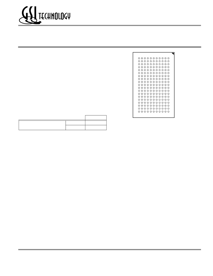
209-Bump, 14 mm x 22 mm BGA
1 mm Bump Pitch, 11 x 19 Bump Array
Bottom View
相關(guān)PDF資料 |
PDF描述 |
|---|---|
| GS8180D18 | 1Mb x 18Bit Separate I/O Sigma DDR SRAM(1M x 18位獨(dú)立I/O接口雙數(shù)據(jù)速率讀和寫模式靜態(tài)ΣRAM) |
| GS8180S36 | 512K x 36Bit Separate I/O Sigma DDR SRAM(512K x 36位獨(dú)立I/O接口雙數(shù)據(jù)速率讀和寫模式靜態(tài)ΣRAM) |
| GS8180S18 | 1Mb x 18Bit Separate I/O Sigma DDR SRAM(1M x 18位獨(dú)立I/O接口雙數(shù)據(jù)速率讀和寫模式靜態(tài)ΣRAM) |
| GS8180S09 | 2Mb x 9Bit Separate I/O Sigma DDR SRAM(2M x 9位獨(dú)立I/O接口雙數(shù)據(jù)速率讀和寫模式靜態(tài)ΣRAM) |
| GS820322T-138 | 64K x 32 2M Synchronous Burst SRAM |
相關(guān)代理商/技術(shù)參數(shù) |
參數(shù)描述 |
|---|---|
| GS8180Q36D-167X | 制造商:GSI Technology 功能描述:512K X 36 (18 MEG)SIGMA QUAD I -SEPERATE I/O BURST OF 2 - Trays |
| GS8180QV36BGD-167 | 制造商:GSI Technology 功能描述:SRAM SYNC DUAL 2.5V 18MBIT 512KX36 2.5NS 165FPBGA - Trays |
| GS8180QV36BGD-167I | 制造商:GSI Technology 功能描述:SRAM SYNC DUAL 2.5V 18MBIT 512KX36 2.5NS 165FPBGA - Trays |
| GS8182D08BD-167 | 制造商:GSI Technology 功能描述:SRAM SYNC DUAL 1.8V 16MBIT 2MX8 0.5NS 165FPBGA - Trays |
| GS8182D08BD-250 | 制造商:GSI Technology 功能描述:SRAM SYNC DUAL 1.8V 16MBIT 2MX8 0.45NS 165FPBGA - Trays |
發(fā)布緊急采購,3分鐘左右您將得到回復(fù)。