- 您現(xiàn)在的位置:買賣IC網(wǎng) > PDF目錄223855 > GLT41116 (Electronic Theatre Controls, Inc.) 64k x 16 CMOS Dynamic RAM with Fast Page Mode PDF資料下載
參數(shù)資料
| 型號(hào): | GLT41116 |
| 廠商: | Electronic Theatre Controls, Inc. |
| 英文描述: | 64k x 16 CMOS Dynamic RAM with Fast Page Mode |
| 中文描述: | 64k的× 16的CMOS動(dòng)態(tài)隨機(jī)存儲(chǔ)器的快速頁(yè)面模式 |
| 文件頁(yè)數(shù): | 11/16頁(yè) |
| 文件大小: | 106K |
| 代理商: | GLT41116 |
第1頁(yè)第2頁(yè)第3頁(yè)第4頁(yè)第5頁(yè)第6頁(yè)第7頁(yè)第8頁(yè)第9頁(yè)第10頁(yè)當(dāng)前第11頁(yè)第12頁(yè)第13頁(yè)第14頁(yè)第15頁(yè)第16頁(yè)

4
G-LINK Technology
GLT41116
July 1998 (Rev. 1)
ELECTRICAL SPECIFICATIONS
1. Stresses greater than those listed under “Absolute Maximum Ratings” may cause permanent damage to the device. This is a stress rating only, and functional operation
of the device at these or any other conditions above those indicated in the operational sections of this specification is not implied. Exposure to absolute maximum rating
conditions for extended periods may affect reliability.
1. Capacitance is sampled and not 100% tested
1. ICC is dependent on output loading when the device output is selected. Specified ICC (max.) is measured with the output open.
2. ICC is dependent upon the number of address transitions specified ICC (max) is measured with a maximum of one transition per address cycle in random READ/WRITE and
Fast-Page Mode.
3. Specified VIL (min) is steady state operation. During transitions VIL (min) may undershoot to -1.0V for a period not to exceed 20 ns. All AC parameter are measured with
VIL (min) ≥ VSS and VIH (max) ≤ VCC.
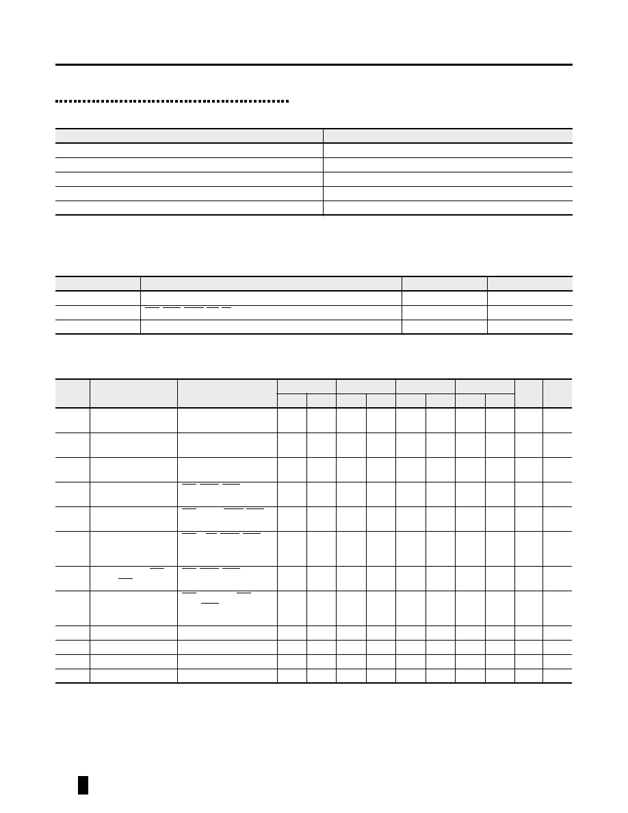
Absolute Maximum Ratings [1]
Parameter
Rating
Operating Temperature, TA (ambient)
-0
°C to +70°C
Storage Temperature (plastic)
-55
°C to +125°C
Voltage Relative to VSS
-1.0V to +7.0V
Short Circuit Output Current‘
50 mA
Power Dissipitation
1.0 W
Capacitance [1]
Symbol
Parameter
Max
Units
CIN1
Address Input
5
pF
CIN2
RAS, LCAS, UCAS, WE, OE
7pF
COUT
Data Input/Output
7
pF
DC Characteristics (TA = 0°C to 70°C, VCC = 5V ± 10%, VSS = 0V, unless otherwise specied)
Symbol
Parameter
Conditions
-30
-35
-40
-45
Units
Notes
Min
Max
Min
Max
Min
Max
Min
Max
ILI
Input Leakage Current
(any input pin)
0V
≤ V
IN ≤ 5.5V (All other
pins not under test = 0V)
-10
+10
-10
+10
-10
+10
-10
+10
A
ILO
Output Leakage Current
(for High-Z State)
0V
≤ V
OUT ≤ 5.5V Output is
disabled (Hiz)
+10
A
ICC1
Operating Current, Ran-
dom READ/WRITE
tRC = tRC (min.)
180
170
160
150
mA
[1] [2]
ICC2
Standby Current, (TTL)
RAS, UCAS, LCAS at VIH
other inputs
≥ V
SS
2222
mA
ICC3
Refresh Current, RAS-
Only
RAS cycling, UCAS, LCAS at
VIH tRC = tRC (min.)
180
170
160
150
mA
[2]
ICC4
Operating Current, EDO
Page Mode
RAS at VIL, UCAS, LCAS
address cycling: tPC = tPC
(min.)
180
170
160
150
mA
[1] [2]
ICC5
Refresh Current, CAS-
before-RAS
RAS, UCAS, LCAS address
cycling: tRC = tRC (min.)
180
170
160
150
mA
[1]
ICC6
Standby Current,
(CMOS)
RAS
≥ V
CC -0.2V, UCS ≥ VCC
-0.2V, LCAS
≥ V
CC -0.2V, All
other inputs
≥ V
CC
2222
mA
VIL
Input Low Voltage
-1
+0.8
-1
+0.8
-1
+0.8
-1
+0.8
V
[3]
VIH
Input High Voltage
2.4
VCC +1
2.4
VCC +1
2.4
VCC +1
2.4
VCC +1
V
VOL
Output Low Voltage
IOL = 4.2 mA
0.4
V
VOH
Output High Voltage
IOH = -5 mA
2.4
V
相關(guān)PDF資料 |
PDF描述 |
|---|---|
| GLZJ18CT/R13 | 17.88 V, 0.5 W, SILICON, UNIDIRECTIONAL VOLTAGE REGULATOR DIODE |
| GLZJ18C | 17.88 V, 0.5 W, SILICON, UNIDIRECTIONAL VOLTAGE REGULATOR DIODE |
| GLZJ2.0BT/R13 | 2.11 V, 0.5 W, SILICON, UNIDIRECTIONAL VOLTAGE REGULATOR DIODE |
| GLZJ2.2AT/R7 | 2.21 V, 0.5 W, SILICON, UNIDIRECTIONAL VOLTAGE REGULATOR DIODE |
| GLZJ2.2BT/R7 | 2.32 V, 0.5 W, SILICON, UNIDIRECTIONAL VOLTAGE REGULATOR DIODE |
相關(guān)代理商/技術(shù)參數(shù) |
參數(shù)描述 |
|---|---|
| GLT4116-30J4 | 制造商:未知廠家 制造商全稱:未知廠家 功能描述:64k x 16 CMOS Dynamic RAM with Fast Page Mode |
| GLT4116-30TC | 制造商:未知廠家 制造商全稱:未知廠家 功能描述:64k x 16 CMOS Dynamic RAM with Fast Page Mode |
| GLT4116-35J4 | 制造商:未知廠家 制造商全稱:未知廠家 功能描述:64k x 16 CMOS Dynamic RAM with Fast Page Mode |
| GLT4116-35TC | 制造商:未知廠家 制造商全稱:未知廠家 功能描述:64k x 16 CMOS Dynamic RAM with Fast Page Mode |
| GLT4116-40J4 | 制造商:未知廠家 制造商全稱:未知廠家 功能描述:64k x 16 CMOS Dynamic RAM with Fast Page Mode |
發(fā)布緊急采購(gòu),3分鐘左右您將得到回復(fù)。