- 您現(xiàn)在的位置:買賣IC網(wǎng) > PDF目錄67592 > FS6131-01G PLL FREQUENCY SYNTHESIZER, 27 MHz, PDSO16 PDF資料下載
參數(shù)資料
| 型號: | FS6131-01G |
| 元件分類: | PLL合成/DDS/VCOs |
| 英文描述: | PLL FREQUENCY SYNTHESIZER, 27 MHz, PDSO16 |
| 封裝: | 0.150 INCH, GREEN, SOP-16 |
| 文件頁數(shù): | 32/40頁 |
| 文件大小: | 746K |
| 代理商: | FS6131-01G |
第1頁第2頁第3頁第4頁第5頁第6頁第7頁第8頁第9頁第10頁第11頁第12頁第13頁第14頁第15頁第16頁第17頁第18頁第19頁第20頁第21頁第22頁第23頁第24頁第25頁第26頁第27頁第28頁第29頁第30頁第31頁當前第32頁第33頁第34頁第35頁第36頁第37頁第38頁第39頁第40頁
38
AMI Semiconductor - Rev. 2.0, Jun. 05
www.amis.com
FS6131-01/FS6131-01g Programmable Line Lock Clock Generator IC
Data Sheet
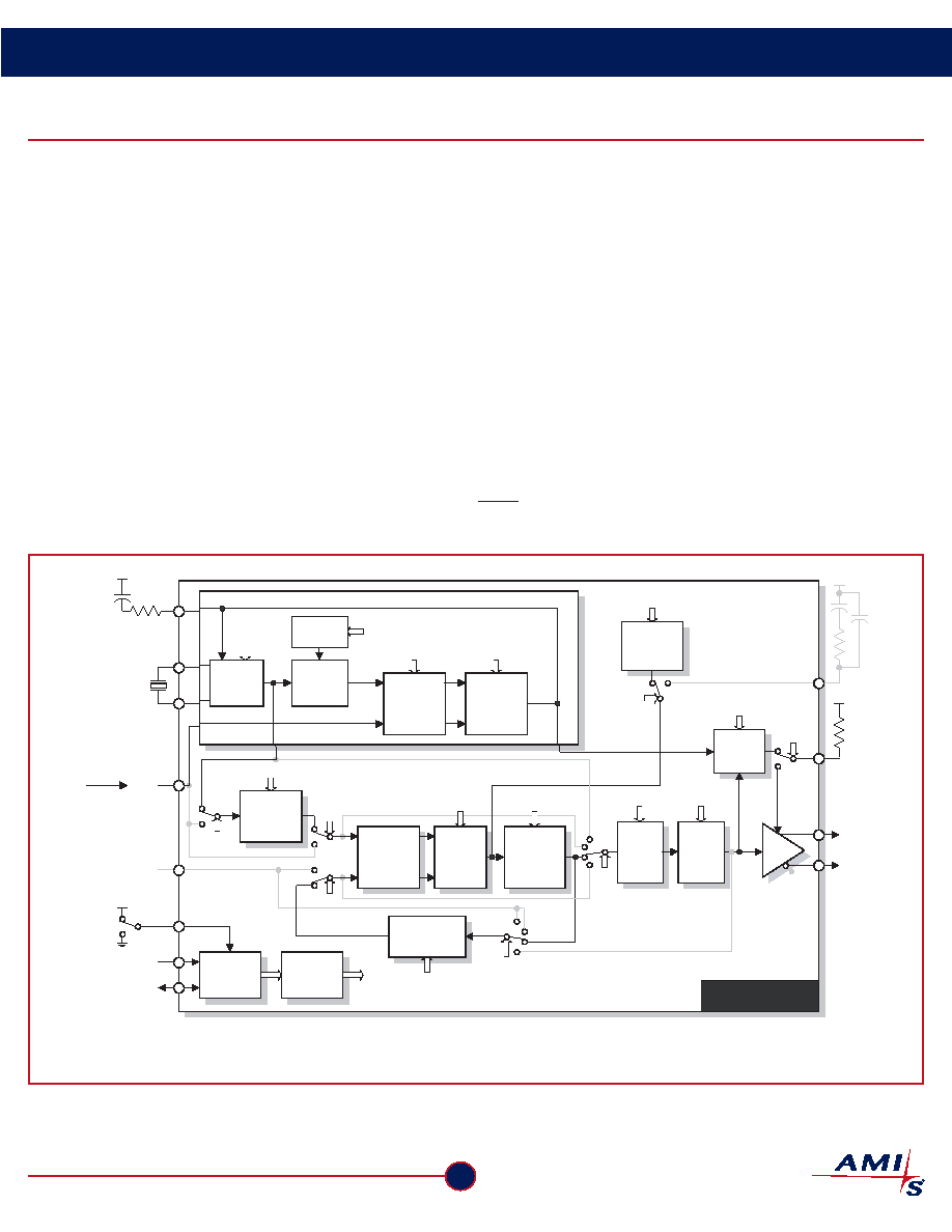
15.0 Device Application: Telecom Clock Regenerator
15.1 Example Calculation
The FS6131 can be used as a clock regenerator as shown in Figure 28. This mode uses the VCXO in its own phase-locked loop, referred to as
the crystal loop. The VCXO provides a "de-jittered" multiple of the reference frequency at the REF pin (usually 8kHz in telecom applications) for
use by the main loop. In essence, the crystal loop "cleans up" the reference signal for the main loop.
The control ROM for the VCXO divider is preloaded with the most common ratios to permit locking of most standard telecommunications crystals
to an 8kHz signal applied to the REF pin. The de-jittered multiple of the reference frequency from the VCXO is then supplied to the reference
divider in the main loop. The reference divider, along with the feedback divider, can be programmed to achieve the desired output clock frequency.
A Visual BASIC program is available to completely program the FS6131 based on the given parameters.
In this example, an 8kHz reference frequency is supplied to the FS6131 and an output clock frequency of 51.84MHz is desired.
First, select the frequency at which the VCXO will operate from Table 10. The table shows the external crystal frequency options available to
choose from, since the VCXO runs at the crystal frequency. While the main loop can be programmed to work with any of the frequencies in the
table, the best performance will be achieved with the highest frequency at the main loop PFD.
The frequency at the main loop PFD (fMLpfd) is the VCXO frequency (fVCXO) divided by the main loop reference divider (NR).
R
VCXO
MLpfd
N
f
=
8kHz IN
(typical)
FS6131
VCXO
Divider
(optional)
CRYSTAL LOOP
MAIN LOOP
VCXO
XOUT
XIN
Control
ROM
XTUNE
Reference
Divider
(N
R)
Phase-
Frequency
Detector
Charge
Pump
UP
DOWN
REF
FBK
Phase-
Frequency
Detector
Charge
Pump
UP
DOWN
Feedback
Divider (N
F)
Internal
Loop
Filter
EXTLF
I2C
Interface
SCL
SDA
ADDR
Registers
POST3[1:0],
POST2[1:0],
POST1[1:0]
REFDIV[11:0]
FBKDIV[14:0]
EXTLF
PDREF
PDFBK
VCOSPD,
OSCTYPE
LFTC
MLCP[1:0]
XLCP[1:0]
XLROM[2:0]
XLPDEN,
XLSWAP
REFDSRC
XCT[3:0],
XLVTEN
(f
REF)
(f
VCO)
LOCK/
IPRG
Post
Divider
(N
Px)
Voltage
Controlled
Oscillator
Lock
Detect
CMOS
(optional)
STAT[1:0]
OM[1:0]
Clock
Gobbler
GBL
(optional)
CMOS/PECL
Output
CLKN
(f
CLK)
CLKP
FBKDSRC[1:0]
R
LF
C
LF
R
IPRG
C
LP
Figure 28: Block Diagram: Telecom Clock Generator
相關PDF資料 |
PDF描述 |
|---|---|
| FS6131-01 | PLL FREQUENCY SYNTHESIZER, 27 MHz, PDSO16 |
| FS6131-01 | PLL FREQUENCY SYNTHESIZER, 27 MHz, PDSO16 |
| FS6S0965R-YDTU | 36 A SWITCHING REGULATOR, 150 kHz SWITCHING FREQ-MAX, PZFM5 |
| FS6S0965R-TU | 36 A SWITCHING REGULATOR, 150 kHz SWITCHING FREQ-MAX, PSFM5 |
| FS6S1265RE-YDTU | 48 A SWITCHING REGULATOR, 150 kHz SWITCHING FREQ-MAX, PZFM5 |
相關代理商/技術參數(shù) |
參數(shù)描述 |
|---|---|
| FS6131-01G-XTD | 功能描述:時鐘發(fā)生器及支持產(chǎn)品 I2C PROG PLL CLK RoHS:否 制造商:Silicon Labs 類型:Clock Generators 最大輸入頻率:14.318 MHz 最大輸出頻率:166 MHz 輸出端數(shù)量:16 占空比 - 最大:55 % 工作電源電壓:3.3 V 工作電源電流:1 mA 最大工作溫度:+ 85 C 安裝風格:SMD/SMT 封裝 / 箱體:QFN-56 |
| FS6131-01G-XTP | 功能描述:時鐘發(fā)生器及支持產(chǎn)品 I2C PROG PLL CLK RoHS:否 制造商:Silicon Labs 類型:Clock Generators 最大輸入頻率:14.318 MHz 最大輸出頻率:166 MHz 輸出端數(shù)量:16 占空比 - 最大:55 % 工作電源電壓:3.3 V 工作電源電流:1 mA 最大工作溫度:+ 85 C 安裝風格:SMD/SMT 封裝 / 箱體:QFN-56 |
| FS6131-01I-XTD | 功能描述:時鐘發(fā)生器及支持產(chǎn)品 I2C PROG PLL CLK (IND) RoHS:否 制造商:Silicon Labs 類型:Clock Generators 最大輸入頻率:14.318 MHz 最大輸出頻率:166 MHz 輸出端數(shù)量:16 占空比 - 最大:55 % 工作電源電壓:3.3 V 工作電源電流:1 mA 最大工作溫度:+ 85 C 安裝風格:SMD/SMT 封裝 / 箱體:QFN-56 |
| FS6131-01I-XTP | 功能描述:時鐘發(fā)生器及支持產(chǎn)品 I2C PROG PLL CLK IND RoHS:否 制造商:Silicon Labs 類型:Clock Generators 最大輸入頻率:14.318 MHz 最大輸出頻率:166 MHz 輸出端數(shù)量:16 占空比 - 最大:55 % 工作電源電壓:3.3 V 工作電源電流:1 mA 最大工作溫度:+ 85 C 安裝風格:SMD/SMT 封裝 / 箱體:QFN-56 |
| FS6186-16/24 | 制造商:Schaffner 功能描述: |
發(fā)布緊急采購,3分鐘左右您將得到回復。