- 您現(xiàn)在的位置:買賣IC網(wǎng) > PDF目錄67592 > FS6131-01 PLL FREQUENCY SYNTHESIZER, 27 MHz, PDSO16 PDF資料下載
參數(shù)資料
| 型號(hào): | FS6131-01 |
| 元件分類: | PLL合成/DDS/VCOs |
| 英文描述: | PLL FREQUENCY SYNTHESIZER, 27 MHz, PDSO16 |
| 封裝: | 0.150 INCH, SOP-16 |
| 文件頁數(shù): | 25/40頁 |
| 文件大小: | 746K |
| 代理商: | FS6131-01 |
第1頁第2頁第3頁第4頁第5頁第6頁第7頁第8頁第9頁第10頁第11頁第12頁第13頁第14頁第15頁第16頁第17頁第18頁第19頁第20頁第21頁第22頁第23頁第24頁當(dāng)前第25頁第26頁第27頁第28頁第29頁第30頁第31頁第32頁第33頁第34頁第35頁第36頁第37頁第38頁第39頁第40頁
31
AMI Semiconductor - Rev. 2.0, Jun. 05
www.amis.com
FS6131-01/FS6131-01g Programmable Line Lock Clock Generator IC
Data Sheet
However, the full signal amplitude may take up to twice as long as the propagation delay of the line to develop, reducing noise immunity during
the half-amplitude period. Note that the voltage at the receive end must add up to a signal amplitude that meets the receiver switching thresholds.
The slew rate of the signal may be reduced due to the additional RC delay of the load capacitance and the line impedance. Also, note that the
output driver impedance will vary slightly with the output logic state (high or low).
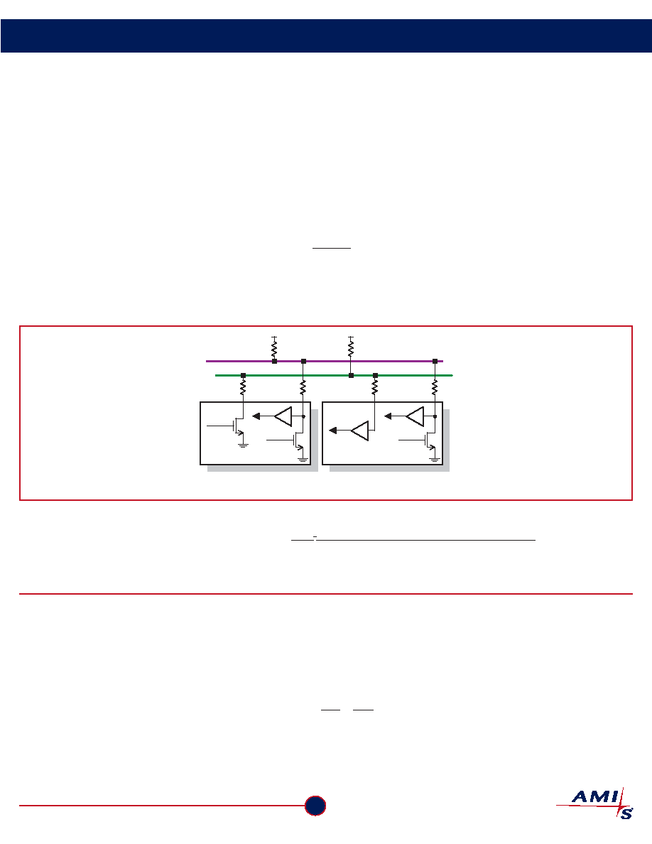
11.3 Serial Communications
Connection of devices to a standard-mode implementation of the I
2C-bus is similar to that shown in Figure 24. Selection of the pull-up resistors
(RP) and the optional series resistors (RS) on the SDA and SCL lines depends on the supply voltage, the bus capacitance and the number of
connected devices with their associated input currents.
Control of the clock and data lines is done through open drain/collector current-sink outputs, and thus requires external pull-up resistors on both
lines.
A guideline is
bus
r
P
C
t
R
<
2
where tr is the maximum rise time (minus some margin) and Cbus is the total bus capacitance. Assuming an I
2C controller and eight to ten other
devices on the bus, including this one, results in values in the 5k
W to 7kW range. Use of a series resistor to provide protection against high voltage
spikes on the bus will alter the values for RP.
R
P
SDA
SCL
Data In
Data Out
Clock Out
TRANSMITTER
Data In
Data Out
RECEIVER
Clock In
R
P
R
S
(optional)
R
S
(optional)
R
S
(optional)
R
S
(optional)
Figure 24: Connections to the Serial Bus
11.3.1 For More Information
More information on the I
2C-bus can be found in the document The I2C-bus And How To Use It (Including Specifications), available from Philips
Semiconductors at http://www-us2.semiconductors.philips.com.
12.0 Device Application: Stand-Alone Clock Generation
The length of the reference and feedback dividers, their granularity and the flexibility of the post divider make the FS6131 the most flexible
monolithic stand-alone PLL clock generation device available. The effective block diagram of the FS6131 when programmed for stand-alone mode
is shown in Figure 25.
The source of the feedback divider in the stand-alone mode is the output of the VCO. By dividing the input reference frequency down by reference
divider (NR), then multiplying it up in the main loop through the feedback divider (NF), and finally dividing the main loop output frequency by the
post divider (NPx), we have the defining relationship for this mode. The equation for the output clock frequency (fCLK) can be written as
÷÷
è
÷÷
è
=
Px
R
F
REF
CLK
N
f
1
where the reference source frequency (fREF) can be either supplied by the VCXO or applied to the REF pin.
Great flexibility is permitted in the programming of the FS6131 to achieve exact desired output frequencies since three integers are involved in
the computation.
(Eqn. 1)
相關(guān)PDF資料 |
PDF描述 |
|---|---|
| FS6131-01 | PLL FREQUENCY SYNTHESIZER, 27 MHz, PDSO16 |
| FS6S0965R-YDTU | 36 A SWITCHING REGULATOR, 150 kHz SWITCHING FREQ-MAX, PZFM5 |
| FS6S0965R-TU | 36 A SWITCHING REGULATOR, 150 kHz SWITCHING FREQ-MAX, PSFM5 |
| FS6S1265RE-YDTU | 48 A SWITCHING REGULATOR, 150 kHz SWITCHING FREQ-MAX, PZFM5 |
| FS6S1265RB-YDTU | 48 A SWITCHING REGULATOR, 150 kHz SWITCHING FREQ-MAX, PZFM5 |
相關(guān)代理商/技術(shù)參數(shù) |
參數(shù)描述 |
|---|---|
| FS6131-01G | 制造商:ONSEMI 制造商全稱:ON Semiconductor 功能描述:Programmable Line Lock Clock Generator IC |
| FS6131-01G-XTD | 功能描述:時(shí)鐘發(fā)生器及支持產(chǎn)品 I2C PROG PLL CLK RoHS:否 制造商:Silicon Labs 類型:Clock Generators 最大輸入頻率:14.318 MHz 最大輸出頻率:166 MHz 輸出端數(shù)量:16 占空比 - 最大:55 % 工作電源電壓:3.3 V 工作電源電流:1 mA 最大工作溫度:+ 85 C 安裝風(fēng)格:SMD/SMT 封裝 / 箱體:QFN-56 |
| FS6131-01G-XTP | 功能描述:時(shí)鐘發(fā)生器及支持產(chǎn)品 I2C PROG PLL CLK RoHS:否 制造商:Silicon Labs 類型:Clock Generators 最大輸入頻率:14.318 MHz 最大輸出頻率:166 MHz 輸出端數(shù)量:16 占空比 - 最大:55 % 工作電源電壓:3.3 V 工作電源電流:1 mA 最大工作溫度:+ 85 C 安裝風(fēng)格:SMD/SMT 封裝 / 箱體:QFN-56 |
| FS6131-01I-XTD | 功能描述:時(shí)鐘發(fā)生器及支持產(chǎn)品 I2C PROG PLL CLK (IND) RoHS:否 制造商:Silicon Labs 類型:Clock Generators 最大輸入頻率:14.318 MHz 最大輸出頻率:166 MHz 輸出端數(shù)量:16 占空比 - 最大:55 % 工作電源電壓:3.3 V 工作電源電流:1 mA 最大工作溫度:+ 85 C 安裝風(fēng)格:SMD/SMT 封裝 / 箱體:QFN-56 |
| FS6131-01I-XTP | 功能描述:時(shí)鐘發(fā)生器及支持產(chǎn)品 I2C PROG PLL CLK IND RoHS:否 制造商:Silicon Labs 類型:Clock Generators 最大輸入頻率:14.318 MHz 最大輸出頻率:166 MHz 輸出端數(shù)量:16 占空比 - 最大:55 % 工作電源電壓:3.3 V 工作電源電流:1 mA 最大工作溫度:+ 85 C 安裝風(fēng)格:SMD/SMT 封裝 / 箱體:QFN-56 |
發(fā)布緊急采購,3分鐘左右您將得到回復(fù)。