- 您現(xiàn)在的位置:買賣IC網(wǎng) > PDF目錄67505 > FMS9875KGC140X (FAIRCHILD SEMICONDUCTOR CORP) 3-CH 8-BIT PROPRIETARY METHOD ADC, PARALLEL ACCESS, PQFP100 PDF資料下載
參數(shù)資料
| 型號(hào): | FMS9875KGC140X |
| 廠商: | FAIRCHILD SEMICONDUCTOR CORP |
| 元件分類: | ADC |
| 英文描述: | 3-CH 8-BIT PROPRIETARY METHOD ADC, PARALLEL ACCESS, PQFP100 |
| 封裝: | MQFP-100 |
| 文件頁數(shù): | 11/31頁 |
| 文件大?。?/td> | 517K |
| 代理商: | FMS9875KGC140X |
第1頁第2頁第3頁第4頁第5頁第6頁第7頁第8頁第9頁第10頁當(dāng)前第11頁第12頁第13頁第14頁第15頁第16頁第17頁第18頁第19頁第20頁第21頁第22頁第23頁第24頁第25頁第26頁第27頁第28頁第29頁第30頁第31頁
FMS9875
PRODUCT SPECIFICATION
REV. 1.2.15 1/14/02
19
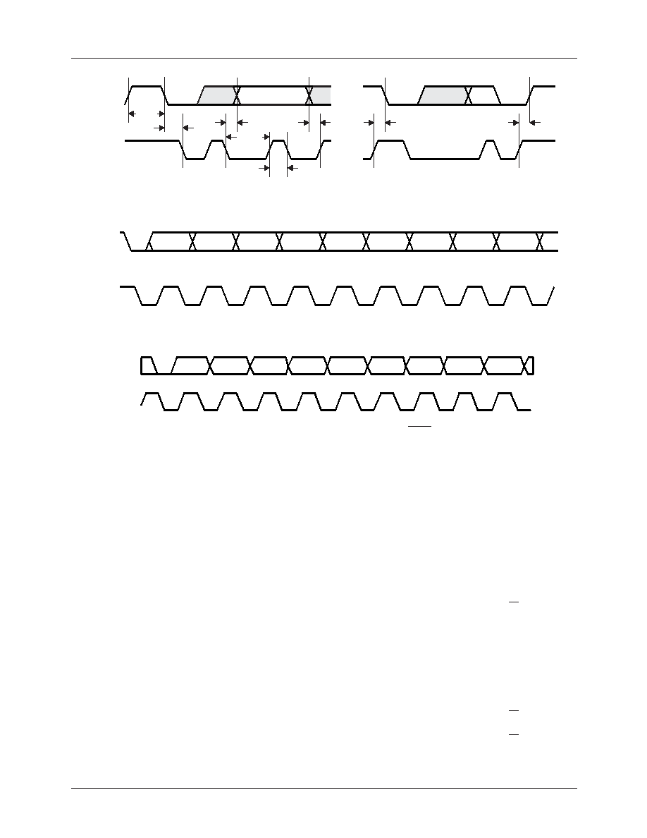
Figure 18. Serial Bus: Read/Write Timing
Figure 19. SerialBus: Typical Byte Transfer
Figure 20. Serial Bus: Slave Address with Read/Write Bit
tBUFF
SDA
SCL
tSTAH
tDHO
tDSU
tDAL
tDAH
tSTASU
tSTOSU
SDA
SCL
bit 7
bit 6
bit 5
bit 4
bit 3
bit 2
bit 1
bit 0
ACK
A6
A5
A4
A3
A2
A1
A0
R/W\
ACK
SDA
SCL
There are ve steps within an I2C/SMBus cycle:
1.
Start signal
2.
Slave address byte
3.
Pointer register address byte
4.
Data byte to read or write
5.
Stop signal
When the Serial Bus interface is inactive, SCL = H and SDA
= H. Communications are initiated by sending a start signal
(Figure 18, left waveform) that is a HIGH-to-LOW transition
on SDA while SCL is HIGH. A start signal alerts all slaved
devices that a data transfer sequence is imminent.
After a start signal, the rst eight bits of data comprise a seven
bit slave address followed a single R/W bit (Read = H, Write
= L) to set the direction of data transfer: read from; or write
to the slave device. If the transmitted slave address matches
the address of the FMS9875 which set by the state of the
ADD pin, the FMS9875 acknowledges by pulling SDA
LOW on the 9th SCL pulse (see Figure 20). If the addresses
do not match or the register being accessed is 0x0F, the
FMS9875 does not acknowledge.
For each byte of data read or written, the MSB is the rst bit
of the sequence.
Data Transfer via Serial Interface
If a slave device, such as the FMS9875 does not acknowl-
edge the master device during a write sequence, SDA
remains HIGH so the master can generate a stop signal. Dur-
ing a read sequence, if the master device does not acknowl-
edge by bringing SDA = L, the FMS9875 interprets SDA =
H as “end of data.” SDA remains HIGH so the master can
generate a stop signal.
To write data to a specic FMS9875 control register, three
bytes are sent:
1.
Write the slave address byte with bit R/W = L.
2.
Write the pointer byte.
3.
Write to the control register indexed by the pointer.
After each byte is written, the pointer auto-increments to
allow multiple data byte transfers within one write cycle.
Data is read from the control registers of the FMS9875 in a simi-
lar manner, except that two data transfer operations are required:
1.
Write the slave address byte with bit R/W = L.
2.
Write the pointer byte.
3.
Write the slave address byte with bit R/W = H
4.
Read the control register indexed by the pointer.
相關(guān)PDF資料 |
PDF描述 |
|---|---|
| FN3410-10-44 | 500 V, 50 HZ, THREE PHASE EMI FILTER |
| FN3410-110-35 | 500 V, 50 HZ, THREE PHASE EMI FILTER |
| FN3410-13-44 | 500 V, 50 HZ, THREE PHASE EMI FILTER |
| FN3410-150-40 | 500 V, 50 HZ, THREE PHASE EMI FILTER |
| FN3410-16-44 | 500 V, 50 HZ, THREE PHASE EMI FILTER |
相關(guān)代理商/技術(shù)參數(shù) |
參數(shù)描述 |
|---|---|
| FMS9875KWC | 制造商:Fairchild Semiconductor Corporation 功能描述: |
| FMS9884A | 制造商:FAIRCHILD 制造商全稱:Fairchild Semiconductor 功能描述:3x8-Bit, 108/140/175 Ms/s Triple Video A/D Converter with Clamps |
| FMS9884AKAC100 | 功能描述:視頻模擬/數(shù)字化轉(zhuǎn)換器集成電路 MQFP RoHS:否 制造商:Texas Instruments 輸入信號(hào)類型:Differential 轉(zhuǎn)換器數(shù)量:1 ADC 輸入端數(shù)量:4 轉(zhuǎn)換速率:3 Gbps 分辨率:8 bit 結(jié)構(gòu): 輸入電壓:3.3 V 接口類型:SPI 信噪比: 電壓參考: 電源電壓-最大:3.45 V 電源電壓-最小:3.15 V 最大功率耗散: 最大工作溫度:+ 85 C 最小工作溫度:- 40 C 封裝 / 箱體:TCSP-48 封裝:Reel |
| FMS9884AKAC140 | 功能描述:視頻模擬/數(shù)字化轉(zhuǎn)換器集成電路 MQFP RoHS:否 制造商:Texas Instruments 輸入信號(hào)類型:Differential 轉(zhuǎn)換器數(shù)量:1 ADC 輸入端數(shù)量:4 轉(zhuǎn)換速率:3 Gbps 分辨率:8 bit 結(jié)構(gòu): 輸入電壓:3.3 V 接口類型:SPI 信噪比: 電壓參考: 電源電壓-最大:3.45 V 電源電壓-最小:3.15 V 最大功率耗散: 最大工作溫度:+ 85 C 最小工作溫度:- 40 C 封裝 / 箱體:TCSP-48 封裝:Reel |
| FMS9884AKAC175 | 功能描述:視頻模擬/數(shù)字化轉(zhuǎn)換器集成電路 MQFP RoHS:否 制造商:Texas Instruments 輸入信號(hào)類型:Differential 轉(zhuǎn)換器數(shù)量:1 ADC 輸入端數(shù)量:4 轉(zhuǎn)換速率:3 Gbps 分辨率:8 bit 結(jié)構(gòu): 輸入電壓:3.3 V 接口類型:SPI 信噪比: 電壓參考: 電源電壓-最大:3.45 V 電源電壓-最小:3.15 V 最大功率耗散: 最大工作溫度:+ 85 C 最小工作溫度:- 40 C 封裝 / 箱體:TCSP-48 封裝:Reel |
發(fā)布緊急采購,3分鐘左右您將得到回復(fù)。