- 您現(xiàn)在的位置:買賣IC網(wǎng) > PDF目錄67505 > FMS9875KGC100X (FAIRCHILD SEMICONDUCTOR CORP) 3-CH 8-BIT PROPRIETARY METHOD ADC, PARALLEL ACCESS, PQFP100 PDF資料下載
參數(shù)資料
| 型號: | FMS9875KGC100X |
| 廠商: | FAIRCHILD SEMICONDUCTOR CORP |
| 元件分類: | ADC |
| 英文描述: | 3-CH 8-BIT PROPRIETARY METHOD ADC, PARALLEL ACCESS, PQFP100 |
| 封裝: | MQFP-100 |
| 文件頁數(shù): | 12/31頁 |
| 文件大?。?/td> | 517K |
| 代理商: | FMS9875KGC100X |
第1頁第2頁第3頁第4頁第5頁第6頁第7頁第8頁第9頁第10頁第11頁當(dāng)前第12頁第13頁第14頁第15頁第16頁第17頁第18頁第19頁第20頁第21頁第22頁第23頁第24頁第25頁第26頁第27頁第28頁第29頁第30頁第31頁
PRODUCT SPECIFICATION
FMS9875
2
REV. 1.2.15 1/14/02
Architectural Overview
Three separate digitizer channels are controlled by common
timing signals derived from the Timing Generator. A/D clock
signals can be derived from either a PLL or an external clock
XCK. With the PLL selected, A/D clocks track the incoming
horizontal sync signal connected to the HSIN input. Setup is
controlled by registers that are accessible through the serial
interface.
Conversion Channels
Typical RGB or YPBPR input signals, GYIN, BPIN, and
RPIN are ground referenced with 700mV amplitude. If a
sync signal is embedded then the usual format is sync on
green or Y with the sync tip at ground, the black level
elevated to 300mV and peak green at 1000mV. Either type
of input can be accepted by using the clamp function with
AC coupling.
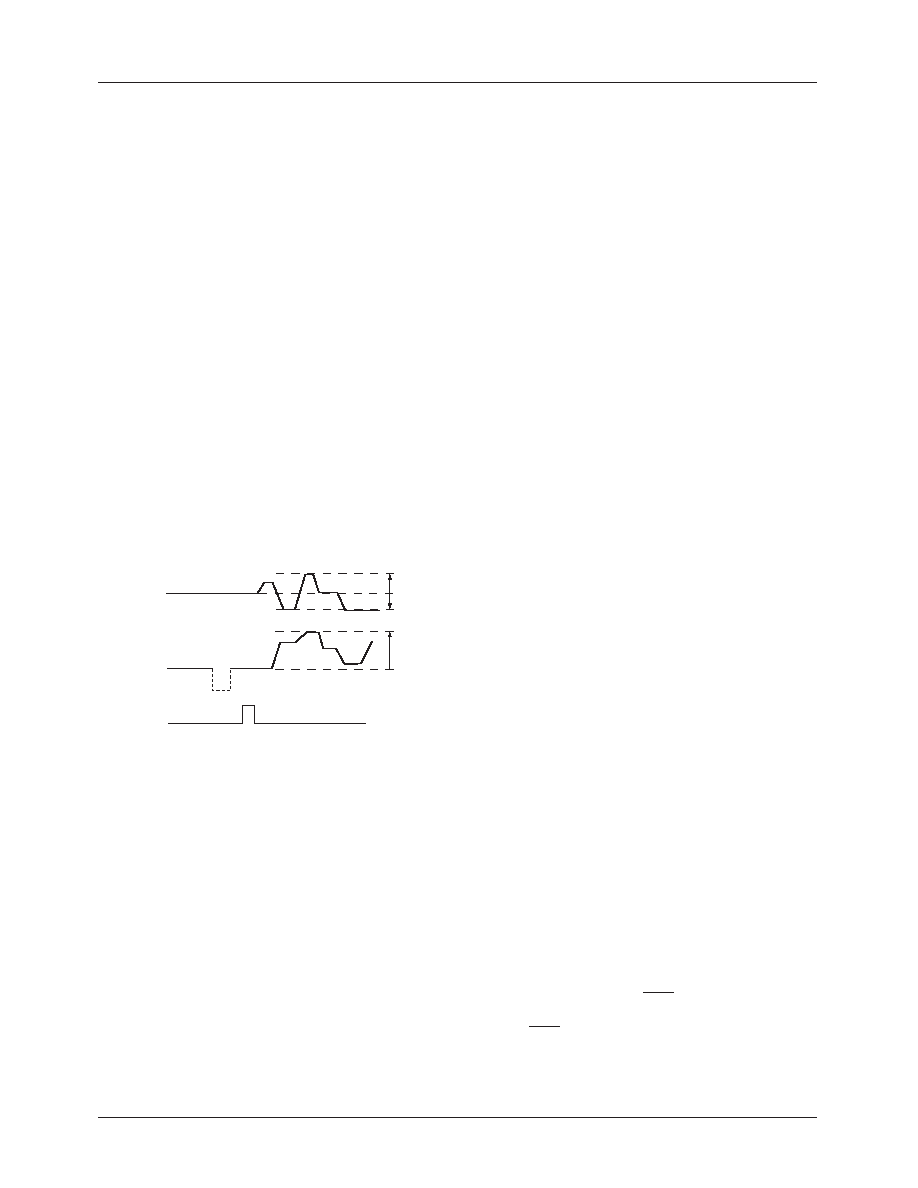
Clamps
AC coupled input video signals must be level shifted to
match the signal and A/D converter reference levels during
the back porch (see Figure 1). Y/G inputs should be clamped
to the A/D converter lower reference level. PBPR signals
should be clamped to the A/D converter midrange level
(nominally 350 mV), which is 50% of full scale (nominally
700 mV).
Figure 1. Clamping to the back-porch
Clamp pulses, ICLAMP, are derived from internal Timing
and Control logic or from the external CLAMP input. Clamp
timing is common to the three input channels.
With the A/D range set to 700mV ground referenced, clamp
levels are:
RGB: 000mV
Y: 000mV
PBPR: +350mV
Clamp levels can be set through the registers or through the
YGREF, BPREF and RPREF pins.
Gain and Offset
Gain and Offset registers serve two functions: 1) Adjustment
of contrast and brightness by setting RGB values in tandems.
2) Matching the gain and offsets between channels, by
setting RGB values individually to obtain the same output
levels at zero and full-scale.
A/D conversion range can be matched to the amplitude of the
incoming video signal by programming Gain Registers
GGY, GBP and GRP, which vary sensitivity (LSB/volt) over
a 2:1 range. Incoming video signal amplitudes varying from
0.5 to 1.0 volt can be accommodated.
Input offset voltage of each converter is programmable in 1
LSB steps through the 6-bit OSGY, OSBP and OSRP regis-
ters. Range of adjustment is equivalent to –31 to +32 LSB.
A/D Converter
Each A/D converter digitizes the analog input into 8-bit data
words. Latency is 5–51/2 clock cycles, depending upon the
state of the INVSCK pin.
VREFIN is the source of reference voltage for the three A/D
converters. VREFIN can be connected to either the internal
bandgap voltage, VREFOUT or an external voltage.
Output Data Conguration
For RGB outputs, data format is unsigned binary: 00
corresponds to the lowest input; FF corresponds to the
highest input.
For YPBPR outputs, the data format is:
Y (0 to 700mV input): unsigned binary.
PBPR (±350mV input): twos-complement or offset binary.
Output data format is:
24-bit YPBPR444
16-bit YPBPR422
With 422 sampling, PBPR samples are coincident with even
samples of Y, beginning with 0.
HSOUT, L-to-H transition identies the rst sample.
Timing and Control
Timing and Control logic encompasses the Timing Generator,
PLL and Serial Interface.
Timing Generator
All internal clock and synchronization signals are generated
by the Timing Generator. Master Clock source is either the
PLL or the external clock input, XCK. Register bit, XCKSEL
selects the Master Clock source. Two clocks are generated.
Sampling clock, SCK is supplied to all three A/D converters.
Phase of SCK (relative to HSIN) can be adjusted in 32 11.25
degree phase increments using the 5-bit PHASE register.
Output data clocks, DCK and DCK are provided for
synchronizing data transfer from the digitizer outputs.
DCK and DCK are slaved to SCK.
Incoming horizontal sync HSIN is propagated by the Timing
and Control to HSOUT with a delay that aligns the leading
edge with the output data.
YGIN
+350 mV
-350 mV
+700 mV
PBIN, PRIN
ICLAMP
相關(guān)PDF資料 |
PDF描述 |
|---|---|
| FMS9875KGC140 | 3-CH 8-BIT PROPRIETARY METHOD ADC, PARALLEL ACCESS, PQFP100 |
| FMS9875KGC140X | 3-CH 8-BIT PROPRIETARY METHOD ADC, PARALLEL ACCESS, PQFP100 |
| FN3410-10-44 | 500 V, 50 HZ, THREE PHASE EMI FILTER |
| FN3410-110-35 | 500 V, 50 HZ, THREE PHASE EMI FILTER |
| FN3410-13-44 | 500 V, 50 HZ, THREE PHASE EMI FILTER |
相關(guān)代理商/技術(shù)參數(shù) |
參數(shù)描述 |
|---|---|
| FMS9875KGC140 | 制造商:未知廠家 制造商全稱:未知廠家 功能描述: |
| FMS9875KGC140X | 制造商:未知廠家 制造商全稱:未知廠家 功能描述: |
| FMS9875KWC | 制造商:Fairchild Semiconductor Corporation 功能描述: |
| FMS9884A | 制造商:FAIRCHILD 制造商全稱:Fairchild Semiconductor 功能描述:3x8-Bit, 108/140/175 Ms/s Triple Video A/D Converter with Clamps |
| FMS9884AKAC100 | 功能描述:視頻模擬/數(shù)字化轉(zhuǎn)換器集成電路 MQFP RoHS:否 制造商:Texas Instruments 輸入信號類型:Differential 轉(zhuǎn)換器數(shù)量:1 ADC 輸入端數(shù)量:4 轉(zhuǎn)換速率:3 Gbps 分辨率:8 bit 結(jié)構(gòu): 輸入電壓:3.3 V 接口類型:SPI 信噪比: 電壓參考: 電源電壓-最大:3.45 V 電源電壓-最小:3.15 V 最大功率耗散: 最大工作溫度:+ 85 C 最小工作溫度:- 40 C 封裝 / 箱體:TCSP-48 封裝:Reel |
發(fā)布緊急采購,3分鐘左右您將得到回復(fù)。