- 您現(xiàn)在的位置:買(mǎi)賣(mài)IC網(wǎng) > PDF目錄377114 > FLEX10KA (Altera Corporation) Embedded Programmable Logic Family PDF資料下載
參數(shù)資料
| 型號(hào): | FLEX10KA |
| 廠(chǎng)商: | Altera Corporation |
| 英文描述: | Embedded Programmable Logic Family |
| 中文描述: | 嵌入式可編程邏輯系列 |
| 文件頁(yè)數(shù): | 113/114頁(yè) |
| 文件大?。?/td> | 1422K |
| 代理商: | FLEX10KA |
第1頁(yè)第2頁(yè)第3頁(yè)第4頁(yè)第5頁(yè)第6頁(yè)第7頁(yè)第8頁(yè)第9頁(yè)第10頁(yè)第11頁(yè)第12頁(yè)第13頁(yè)第14頁(yè)第15頁(yè)第16頁(yè)第17頁(yè)第18頁(yè)第19頁(yè)第20頁(yè)第21頁(yè)第22頁(yè)第23頁(yè)第24頁(yè)第25頁(yè)第26頁(yè)第27頁(yè)第28頁(yè)第29頁(yè)第30頁(yè)第31頁(yè)第32頁(yè)第33頁(yè)第34頁(yè)第35頁(yè)第36頁(yè)第37頁(yè)第38頁(yè)第39頁(yè)第40頁(yè)第41頁(yè)第42頁(yè)第43頁(yè)第44頁(yè)第45頁(yè)第46頁(yè)第47頁(yè)第48頁(yè)第49頁(yè)第50頁(yè)第51頁(yè)第52頁(yè)第53頁(yè)第54頁(yè)第55頁(yè)第56頁(yè)第57頁(yè)第58頁(yè)第59頁(yè)第60頁(yè)第61頁(yè)第62頁(yè)第63頁(yè)第64頁(yè)第65頁(yè)第66頁(yè)第67頁(yè)第68頁(yè)第69頁(yè)第70頁(yè)第71頁(yè)第72頁(yè)第73頁(yè)第74頁(yè)第75頁(yè)第76頁(yè)第77頁(yè)第78頁(yè)第79頁(yè)第80頁(yè)第81頁(yè)第82頁(yè)第83頁(yè)第84頁(yè)第85頁(yè)第86頁(yè)第87頁(yè)第88頁(yè)第89頁(yè)第90頁(yè)第91頁(yè)第92頁(yè)第93頁(yè)第94頁(yè)第95頁(yè)第96頁(yè)第97頁(yè)第98頁(yè)第99頁(yè)第100頁(yè)第101頁(yè)第102頁(yè)第103頁(yè)第104頁(yè)第105頁(yè)第106頁(yè)第107頁(yè)第108頁(yè)第109頁(yè)第110頁(yè)第111頁(yè)第112頁(yè)當(dāng)前第113頁(yè)第114頁(yè)
Altera Corporation
113
FLEX 10K Embedded Programmable Logic Family Data Sheet
Notes to tables:
(1)
All pins that are not listed are user I/O pins.
(2)
Pin-out information on FLEX 10KA devices (except EPF10K50V, EPF10K130V, and EPF10K100A devices) and
FLEX 10KB devices are preliminary. Contact Altera Applications for the latest pin-out information.
(3)
This pin is a dedicated pin; it is not available as a user I/O pin.
(4)
This pin can be used as a user I/O pin if it is not used for its device-wide or configuration function.
(5)
This pin can be used as a user I/O pin after configuration.
(6)
This pin is tri-stated in user mode.
(7)
The optional JTAG pin
TRST
is not used in the 144-pin TQFP package.
(8)
To maintain pin compatibility when transferring to the EPF10K10 device from any other device in the 208-pin PQFP
package, do not use these pins as user I/O pins.
(9)
The user I/O pin count includes dedicated input pins, dedicated clock pins, and all I/O pins.
(10) To maintain pin compatibility when transferring to the EPF10K30 device from any other device in the 356-pin BGA
package, do not use these pins as user I/O pins.
(11) To maintain pin compatibility when transferring from the EPF10K100 to the EPF10K70 in the 503-pin PGA package,
do not use these pins as user I/O pins.
(12) This pin shows the status of the ClockLock and ClockBoost circuitry. When the ClockLock and ClockBoost circuitry
is locked to the incoming clock and generates an internal clock,
LOCK
is driven high.
LOCK
remains high if a periodic
clock stops clocking. The
LOCK
function is optional; if the
LOCK
output is not used, this pin is a user I/O pin.
(13) This pin drives the ClockLock and ClockBoost circuitry.
(14) To maintain pin compatibility when transferring a to the EPF10K100A device from another device in the 600-pin
BGA package, do not use these pin as user I/O pins.
(15) This pin is the power or ground for the ClockLock and ClockBoost circuitry. To ensure noise resistance, the power
and ground supply to the ClockLock and ClockBoost circuitry should be isolated from the power and ground to the
rest of the device.
No Connect (N.C.)
(14)
–
–
AK5, AL4, AM3, AM2,
AM1, AJ5, AL2, AK4,
AL1, AK3, AJ4, AH5,
AK2, AK1, AJ3, AJ2,
G1, G2, G3, F1, F2,
H5, G4, F3, E1, E3,
F4, G5, D1, D2, D3,
E4, E32, D33, D34,
D35, G31, F32, E33,
E34, E35, F33, G32,
H31, F34, G33, G34,
G35, AB34, AB33,
AB32, AB31, AC35,
AC34, AC33, AC32,
AC31, AD34, AD33,
AD32, AD31, AE35,
AE34, AE33
406
–
Total User I/O Pins
(9)
406
470
470
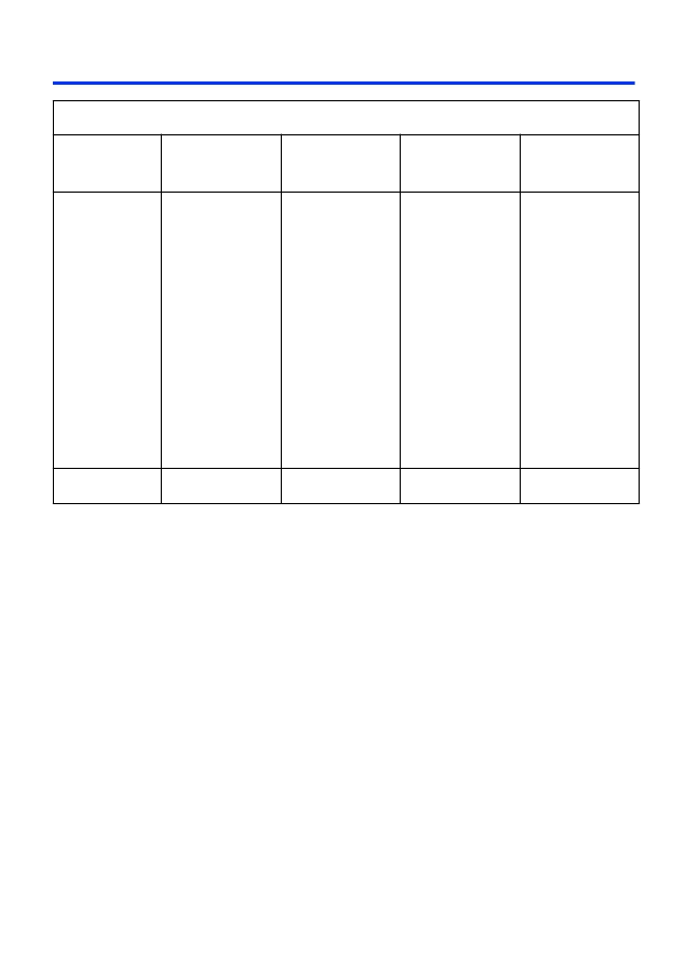
Table 26. FLEX 10K Pin-Outs (Part 3 of 3)
Notes (1), (2)
Pin Name
503-Pin PGA
EPF10K100
599-Pin PGA
EPF10K130V
EPF10K250A
600-Pin BGA
EPF10K100A
600-Pin BGA
EPF10K130V
EPF10K250A
相關(guān)PDF資料 |
PDF描述 |
|---|---|
| FLEX10KE | Embedded Programmable Logic Family |
| FLEX6000 | Programmable Logic Device Family |
| FLEX8000 | PROGRAMMABLE LOGIC DEVICES FAMILY |
| FLL120MK | L-Band Medium & High Power GaAs FET |
| FLL200IB-1 | L-Band Medium & High Power GaAs FET |
相關(guān)代理商/技術(shù)參數(shù) |
參數(shù)描述 |
|---|---|
| FLEX10KE | 制造商:ALTERA 制造商全稱(chēng):Altera Corporation 功能描述:Embedded Programmable Logic Device |
| FLEX110 | 功能描述:開(kāi)發(fā)板和工具包 - PIC / DSPIC Multibus Pack RoHS:否 制造商:Microchip Technology 產(chǎn)品:Starter Kits 工具用于評(píng)估:chipKIT 核心:Uno32 接口類(lèi)型: 工作電源電壓: |
| FLEX111 | 功能描述:開(kāi)發(fā)板和工具包 - PIC / DSPIC Fasttrack suite RoHS:否 制造商:Microchip Technology 產(chǎn)品:Starter Kits 工具用于評(píng)估:chipKIT 核心:Uno32 接口類(lèi)型: 工作電源電壓: |
| FLEX112 | 功能描述:開(kāi)發(fā)板和工具包 - PIC / DSPIC Demo2 Pack RoHS:否 制造商:Microchip Technology 產(chǎn)品:Starter Kits 工具用于評(píng)估:chipKIT 核心:Uno32 接口類(lèi)型: 工作電源電壓: |
| FLEX113 | 功能描述:開(kāi)發(fā)板和工具包 - 無(wú)線(xiàn) Mini Kit RoHS:否 制造商:Arduino 產(chǎn)品:Evaluation Boards 工具用于評(píng)估:AT32UC3L 核心:AVR32 頻率: 接口類(lèi)型:USB 工作電源電壓:5 V |
發(fā)布緊急采購(gòu),3分鐘左右您將得到回復(fù)。