- 您現(xiàn)在的位置:買賣IC網(wǎng) > Datasheet目錄38 > FAN6920MRMY (Fairchild Semiconductor)IC PWM CTLR PFC/QUASI-RES 16SOP Datasheet資料下載
參數(shù)資料
| 型號: | FAN6920MRMY |
| 廠商: | Fairchild Semiconductor |
| 文件頁數(shù): | 17/24頁 |
| 文件大小: | 1490K |
| 描述: | IC PWM CTLR PFC/QUASI-RES 16SOP |
| 標(biāo)準(zhǔn)包裝: | 1 |
| 模式: | 臨界傳導(dǎo)(CRM) |
| 電流 - 啟動: | 20µA |
| 電源電壓: | 12 V ~ 25 V |
| 工作溫度: | -40°C ~ 105°C |
| 安裝類型: | 表面貼裝 |
| 封裝/外殼: | 16-SOIC(0.154",3.90mm 寬) |
| 供應(yīng)商設(shè)備封裝: | 16-SOP |
| 包裝: | 標(biāo)準(zhǔn)包裝 |
| 其它名稱: | FAN6920MRMYDKR |
?2010 Fairchild Semiconductor Corporation
www.fairchildsemi.com
FAN6920MR " Rev. 1.0.8
17
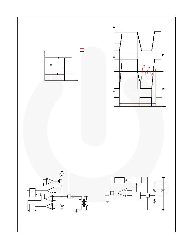
RANGE Pin
A built-in low-voltage MOSFET can be turned on or off
according to V
VIN
voltage level and PFC status. The
drain pin of this internal MOSFET is connected to the
RANGE pin. Figure 29 shows the status curve of V
VIN
voltage level and RANGE impedance (open or ground).
V
VIN
RANGE=
Ground
V
VIN-RANGE-L
V
VIN-RANGE-H
RANGE=
Open
PFC Normal Mode Condition
PFC Burst Mode Condition
Figure 29. Hysteresis Behavior between RANGE Pin
and VIN Pin Voltage
Zero-Current Detection (ZCD Pin)
Figure 30 shows the internal block of zero-current
detection. The detection function is performed by
sensing the information on an auxiliary winding of the
PFC inductor. Referring to Figure 31, when PFC MOS is
off, the stored energy of the PFC inductor starts to
release to the output load. Then the drain voltage of
PFC MOS starts to decrease since the PFC inductor
resonates with parasitic capacitance. Once the ZCD pin
voltage is lower than the triggering voltage (1.75 V
typical), the PFC gate signal is sent again to start a new
switching cycle.
If PFC operation needs to be shut down due to
abnormal condition, pull the ZCD pin LOW, voltage
under 0.2 V (typical), to activate the PFC disable
function to stop PFC switching operation.
For preventing excessive high switching frequency at
light load, a built-in inhibit timer is used to limit the
minimum t
OFF
time. Even if the ZCD signal has been
detected, the PFC gate signal is not sent during the
inhibit time (2.5 祍 typical).
5
1 0 V
1 .7 5 V
Z C D
FA N 6 9 2 0 M R
1 :n
V
AC
L
b
0 .2 5 V
PF C G a te O n
2 .1 V
R
S
Q
P F C G a te
D riv e
R
S
Q
R
Z C D
0 .2 V
Figure 30. Internal Block of the Zero-Current
Detection
V
ZCD
PFC
G ate
V
IN,M AX
PFCVO
V
DS
10V
2.1V
1.75V
Inhibit
Tim e
t
t
t
Figure 31. Operation Waveforms of PFC
Zero-Current Detection
Protection for PFC Stage
PFC Output Voltage UVP and OVP (INV Pin)
FAN6920MR provides several kinds of protection for
PFC stage. PFC output over- and under-voltage are
essential for PFC stage. Both are detected and
determined by INV pin voltage, as shown in Figure 32.
When INV pin voltage is over 2.75 V or under 0.45 V,
due to overshoot or abnormal conditions, and lasts for a
de-bounce time around 70 祍; the OVP or UVP circuit is
activated to stop PFC switching operation immediately.
The INV pin is not only used to receive and regulate
PFC output voltage; it can also perform PFC output
OVP/ UVP protection. For failure-mode test, this pin can
shut down PFC switching if pin floating occurs.
3
2
V
c o m p
E r r o r
A m p lif ie r
C O M P
F A N 6 9 2 0 M R
O V P = (V
IN V
e 2 .7 5 V )
U V P = (V
I N V
d 0 .4 5 V )
V o lt a g e
D e t e c t o r
IN V
C
O
V
O
D e b o u n c e
T im e
D r iv e r
V
R E F
( 2 . 5 V )
c o m p
Figure 32. Internal Block of PFC Over-
and Under-Voltage Protection
相關(guān)PDF資料 |
PDF描述 |
|---|---|
| FAN6921MLMY | IC CTLR PFC/FLYBACK 16-SOICN |
| FAN6921MRMY | IC CTLR PFC/FLYBACK 16-SOICN |
| FAN6961SZ | IC PFC CONTROLLER DCM 8SOP |
| FAN6982MY | IC CTLR PFC CCM 14-SOICN |
| FAN7527BN | IC PFC CTRLR TRANSITION 8DIP |
相關(guān)代理商/技術(shù)參數(shù) |
參數(shù)描述 |
|---|---|
| FAN6921 | 制造商:Fairchild Semiconductor Corporation 功能描述: |
| FAN6921AMLMY | 功能描述:電流型 PWM 控制器 PFC/Quasi-Resonant PWM Controller RoHS:否 制造商:Texas Instruments 開關(guān)頻率:27 KHz 上升時間: 下降時間: 工作電源電壓:6 V to 15 V 工作電源電流:1.5 mA 輸出端數(shù)量:1 最大工作溫度:+ 105 C 安裝風(fēng)格:SMD/SMT 封裝 / 箱體:TSSOP-14 |
| FAN6921AMRMY | 功能描述:功率因數(shù)校正 IC Integrated CRM PFC QR Flyback controler RoHS:否 制造商:Fairchild Semiconductor 開關(guān)頻率:300 KHz 最大功率耗散: 最大工作溫度:+ 125 C 安裝風(fēng)格:SMD/SMT 封裝 / 箱體:SOIC-8 封裝:Reel |
| FAN6921ML | 制造商:FAIRCHILD 制造商全稱:Fairchild Semiconductor 功能描述:Integrated Critical Mode PFC/Quasi-Resonant Current Mode PWM Controller |
| FAN6921MLMY | 功能描述:電流型 PWM 控制器 Critical Mode PFC Quasi-Resant PWM cnt RoHS:否 制造商:Texas Instruments 開關(guān)頻率:27 KHz 上升時間: 下降時間: 工作電源電壓:6 V to 15 V 工作電源電流:1.5 mA 輸出端數(shù)量:1 最大工作溫度:+ 105 C 安裝風(fēng)格:SMD/SMT 封裝 / 箱體:TSSOP-14 |
發(fā)布緊急采購,3分鐘左右您將得到回復(fù)。