- 您現(xiàn)在的位置:買賣IC網(wǎng) > PDF目錄362739 > EP1K10 (Altera Corporation) ACEX 1K Programmable Logic Family(ACEX 1K 系列可編程邏輯) PDF資料下載
參數(shù)資料
| 型號: | EP1K10 |
| 廠商: | Altera Corporation |
| 英文描述: | ACEX 1K Programmable Logic Family(ACEX 1K 系列可編程邏輯) |
| 中文描述: | ACEX一千可編程邏輯系列(ACEX每1000系列可編程邏輯) |
| 文件頁數(shù): | 5/84頁 |
| 文件大小: | 1366K |
| 代理商: | EP1K10 |
第1頁第2頁第3頁第4頁當前第5頁第6頁第7頁第8頁第9頁第10頁第11頁第12頁第13頁第14頁第15頁第16頁第17頁第18頁第19頁第20頁第21頁第22頁第23頁第24頁第25頁第26頁第27頁第28頁第29頁第30頁第31頁第32頁第33頁第34頁第35頁第36頁第37頁第38頁第39頁第40頁第41頁第42頁第43頁第44頁第45頁第46頁第47頁第48頁第49頁第50頁第51頁第52頁第53頁第54頁第55頁第56頁第57頁第58頁第59頁第60頁第61頁第62頁第63頁第64頁第65頁第66頁第67頁第68頁第69頁第70頁第71頁第72頁第73頁第74頁第75頁第76頁第77頁第78頁第79頁第80頁第81頁第82頁第83頁第84頁
Altera Corporation
5
Preliminary Information
ACEX 1K Programmable Logic Family Data Sheet
D
13
T
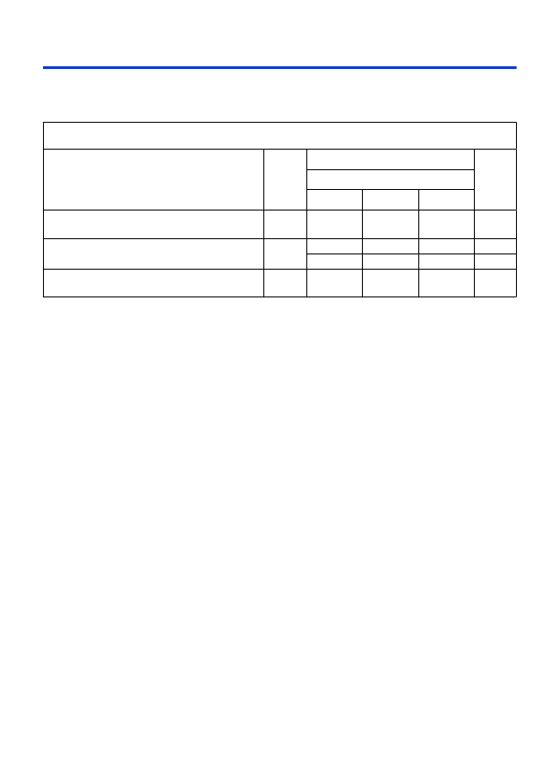
Table 5
shows ACEX 1K device performance for more complex designs.
These designs are available as Altera MegaCore
TM
functions.
Each ACEX 1K device contains an embedded array and a logic array. The
embedded array is used to implement a variety of memory functions or
complex logic functions, such as digital signal processing (DSP), wide
data-path manipulation, microcontroller applications, and data-
transformation functions. The logic array performs the same function as
the sea-of-gates in the gate array and is used to implement general logic
such as counters, adders, state machines, and multiplexers. The
combination of embedded and logic arrays provides the high
performance and high density of embedded gate arrays, enabling
designers to implement an entire system on a single device.
ACEX 1K devices are configured at system power-up with data stored in
an Altera serial configuration device or provided by a system controller.
Altera offers EPC1, EPC2, and EPC1441 configuration devices, which
configure ACEX 1K devices via a serial data stream. Configuration data
can also be downloaded from system RAM or via the Altera
MasterBlaster
TM
, ByteBlasterMV
TM
, ByteBlaster
TM
, or BitBlaster
TM
download cables. (The ByteBlaster cable is obsolete and is replaced by the
ByteBlasterMV
cable, which can program and configure 2.5-V, 3.3-V, and
5.0-V devices.) After an ACEX 1K device has been configured, it can be
reconfigured in-circuit by resetting the device and loading new data.
Because reconfiguration requires less than 40 ms, real-time changes can be
made during system operation.
ACEX 1K devices contain an interface that permits microprocessors to
configure ACEX 1K devices serially or in parallel, and synchronously or
asynchronously. The interface also enables microprocessors to treat an
ACEX 1K device as memory and configure it
by writing to a virtual
memory location, simplifying device reconfiguration.
Table 5. ACEX 1K Device Performance for Complex Designs
Application
LEs
Used
Performance
Units
Speed Grade
-1
-2
-3
16-bit, 8-tap parallel finite impulse response (FIR)
filter
8-bit, 512-point Fast Fourier transform (FFT)
function
420
185
175
122
MSPS
1,854
47.4
100
66
57.8
82
57
76.5
62
44
μ
s
MHz
MHz
a16450
universal asynchronous
receiver/transmitter (UART)
342
相關PDF資料 |
PDF描述 |
|---|---|
| EP1K30 | ACEX 1K Programmable Logic Family(ACEX 1K 系列可編程邏輯) |
| EP1K50 | ACEX 1K Programmable Logic Family(ACEX 1K 系列可編程邏輯) |
| EP1K30TI144-2 | Dual LDO with Low Noise, Low IQ, and High PSRR; Temperature Range: -40°C to 85°C; Package: 10-DFN |
| EP1K10 | Programmable Logic Device Family |
| EP1K100 | Programmable Logic Device Family |
相關代理商/技術參數(shù) |
參數(shù)描述 |
|---|---|
| EP1K100 | 制造商:未知廠家 制造商全稱:未知廠家 功能描述:Programmable Logic Device Family |
| EP1K100FC256-1 | 功能描述:FPGA - 現(xiàn)場可編程門陣列 FPGA - ACEX 1K 624 LABs 186 IOs RoHS:否 制造商:Altera Corporation 系列:Cyclone V E 柵極數(shù)量: 邏輯塊數(shù)量:943 內(nèi)嵌式塊RAM - EBR:1956 kbit 輸入/輸出端數(shù)量:128 最大工作頻率:800 MHz 工作電源電壓:1.1 V 最大工作溫度:+ 70 C 安裝風格:SMD/SMT 封裝 / 箱體:FBGA-256 |
| EP1K100FC256-1N | 功能描述:FPGA - 現(xiàn)場可編程門陣列 FPGA - ACEX 1K 624 LABs 186 IOs RoHS:否 制造商:Altera Corporation 系列:Cyclone V E 柵極數(shù)量: 邏輯塊數(shù)量:943 內(nèi)嵌式塊RAM - EBR:1956 kbit 輸入/輸出端數(shù)量:128 最大工作頻率:800 MHz 工作電源電壓:1.1 V 最大工作溫度:+ 70 C 安裝風格:SMD/SMT 封裝 / 箱體:FBGA-256 |
| EP1K100FC256-2 | 功能描述:FPGA - 現(xiàn)場可編程門陣列 FPGA - ACEX 1K 624 LABs 186 IOs RoHS:否 制造商:Altera Corporation 系列:Cyclone V E 柵極數(shù)量: 邏輯塊數(shù)量:943 內(nèi)嵌式塊RAM - EBR:1956 kbit 輸入/輸出端數(shù)量:128 最大工作頻率:800 MHz 工作電源電壓:1.1 V 最大工作溫度:+ 70 C 安裝風格:SMD/SMT 封裝 / 箱體:FBGA-256 |
| EP1K100FC256-2N | 功能描述:FPGA - 現(xiàn)場可編程門陣列 FPGA - ACEX 1K 624 LABs 186 IOs RoHS:否 制造商:Altera Corporation 系列:Cyclone V E 柵極數(shù)量: 邏輯塊數(shù)量:943 內(nèi)嵌式塊RAM - EBR:1956 kbit 輸入/輸出端數(shù)量:128 最大工作頻率:800 MHz 工作電源電壓:1.1 V 最大工作溫度:+ 70 C 安裝風格:SMD/SMT 封裝 / 箱體:FBGA-256 |
發(fā)布緊急采購,3分鐘左右您將得到回復。