- 您現(xiàn)在的位置:買(mǎi)賣(mài)IC網(wǎng) > PDF目錄377001 > DSP56F801FA80E (飛思卡爾半導(dǎo)體(中國(guó))有限公司) 16-bit Digital Signal Controllers PDF資料下載
參數(shù)資料
| 型號(hào): | DSP56F801FA80E |
| 廠商: | 飛思卡爾半導(dǎo)體(中國(guó))有限公司 |
| 英文描述: | 16-bit Digital Signal Controllers |
| 中文描述: | 16位數(shù)字信號(hào)控制器 |
| 文件頁(yè)數(shù): | 18/48頁(yè) |
| 文件大?。?/td> | 375K |
| 代理商: | DSP56F801FA80E |
第1頁(yè)第2頁(yè)第3頁(yè)第4頁(yè)第5頁(yè)第6頁(yè)第7頁(yè)第8頁(yè)第9頁(yè)第10頁(yè)第11頁(yè)第12頁(yè)第13頁(yè)第14頁(yè)第15頁(yè)第16頁(yè)第17頁(yè)當(dāng)前第18頁(yè)第19頁(yè)第20頁(yè)第21頁(yè)第22頁(yè)第23頁(yè)第24頁(yè)第25頁(yè)第26頁(yè)第27頁(yè)第28頁(yè)第29頁(yè)第30頁(yè)第31頁(yè)第32頁(yè)第33頁(yè)第34頁(yè)第35頁(yè)第36頁(yè)第37頁(yè)第38頁(yè)第39頁(yè)第40頁(yè)第41頁(yè)第42頁(yè)第43頁(yè)第44頁(yè)第45頁(yè)第46頁(yè)第47頁(yè)第48頁(yè)
56F801 Technical Data, Rev. 16
18
Freescale Semiconductor
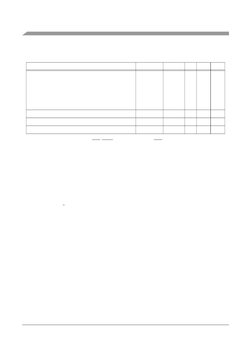
V
DD
supply current
I
DDT6
Run
7
(80MHz operation)
—
120
130
mA
Run
7
(60MHz operation)
—
102
111
mA
Wait
8
—
96
102
mA
Stop
—
62
70
mA
Low Voltage Interrupt, external power supply
9
V
EIO
2.4
2.7
3.0
V
Low Voltage Interrupt, internal power supply
10
V
EIC
2.0
2.2
2.4
V
Power on Reset
11
V
POR
—
1.7
2.0
V
1.
Since the GPIOB[2:3] signals are shared with the XTAL/EXTAL function, these inputs are not 5.5 volt tolerant.
2.
Schmitt Trigger inputs are: FAULTA0, IRQA, RESET, TCS, TCK, TMS, TDI, and TRST.
3.
Analog inputs are: ANA[0:7], XTAL and EXTAL. Specification assumes ADC is not sampling.
4.
PWM pin output source current measured with 50% duty cycle.
5.
PWM pin output sink current measured with 50% duty cycle.
6.
I
DDT
= I
DD
+ I
DDA
(Total supply current for V
DD
+ V
DDA
)
Run (operating) I
DD
measured using 8MHz clock source. All inputs 0.2V from rail; outputs unloaded. All ports configured as
inputs; measured with all modules enabled.
7.
8.
less than 50pF on all outputs. C
L
= 20pF on EXTAL; all ports configured as inputs; EXTAL capacitance linearly affects wait I
DD
;
measured with PLL enabled.
Wait I
DD
measured using external square wave clock source (f
osc
= 8MHz) into XTAL; all inputs 0.2V from rail; no DC loads;
9.
via separate traces. If V
DDA
drops below V
EIO
, an interrupt is generated. Functionality of the device is guaranteed under transient
conditions when V
DDA
>V
EIO
(between the minimum specified V
DD
and the point when the V
EIO
interrupt is generated).
10. This low voltage interrupt monitors the internally regulated core power supply. If the output from the internal voltage is regulator
drops below V
EIC
, an interrupt is generated. Since the core logic supply is internally regulated, this interrupt will not be generated
unless the external power supply drops below the minimum specified value (3.0V).
11. Power
–
on reset occurs whenever the internally regulated 2.5V digital supply drops below 1.5V typical. While power is ramping
up, this signal remains active for as long as the internal 2.5V is below 1.5V typical no matter how long the ramp up rate is. The
internally regulated voltage is typically 100 mV less than V
DD
during ramp up until 2.5V is reached, at which time it self regulates.
This low voltage interrupt monitors the V
DDA
external power supply. V
DDA
is generally connected to the same potential as V
DD
Table 3-4 DC Electrical Characteristics (Continued)
Operating Conditions:
V
SS
= V
SSA
= 0 V, V
DD
= V
DDA
= 3.0–3.6V, T
A
= –40
°
to +85
°
C, C
L
≤
50pF
Characteristic
Symbol
Min
Typ
Max
Unit
相關(guān)PDF資料 |
PDF描述 |
|---|---|
| DSP56F801 | 16-bit Hybrid Controller(16位混合控制器) |
| DSP56F803E | 16-bit Digital Signal Controllers |
| DSP56F805E | 16-bit Digital Signal Controllers |
| DSP56F805FV80E | 16-bit Digital Signal Controllers |
| DSP56F805 | 16-bit Hybrid Controller(16位混合控制器) |
相關(guān)代理商/技術(shù)參數(shù) |
參數(shù)描述 |
|---|---|
| DSP56F801FA80E | 制造商:Freescale Semiconductor 功能描述:IC |
| DSP56F801PB | 制造商:MOTOROLA 制造商全稱(chēng):Motorola, Inc 功能描述:16-bit Digital Signal Processor |
| DSP56F802 | 制造商:FREESCALE 制造商全稱(chēng):Freescale Semiconductor, Inc 功能描述:16-bit Digital Signal Controllers |
| DSP56F802PB | 制造商:未知廠家 制造商全稱(chēng):未知廠家 功能描述:56F802 16-Bit Hybrid Controller Product Brief |
| DSP56F802TA60 | 功能描述:數(shù)字信號(hào)處理器和控制器 - DSP, DSC 60Mhz/30MIPS RoHS:否 制造商:Microchip Technology 核心:dsPIC 數(shù)據(jù)總線(xiàn)寬度:16 bit 程序存儲(chǔ)器大小:16 KB 數(shù)據(jù) RAM 大小:2 KB 最大時(shí)鐘頻率:40 MHz 可編程輸入/輸出端數(shù)量:35 定時(shí)器數(shù)量:3 設(shè)備每秒兆指令數(shù):50 MIPs 工作電源電壓:3.3 V 最大工作溫度:+ 85 C 封裝 / 箱體:TQFP-44 安裝風(fēng)格:SMD/SMT |
發(fā)布緊急采購(gòu),3分鐘左右您將得到回復(fù)。