- 您現(xiàn)在的位置:買賣IC網(wǎng) > PDF目錄379101 > CYNSE70032-66BGC (CYPRESS SEMICONDUCTOR CORP) Network Search Engine PDF資料下載
參數(shù)資料
| 型號: | CYNSE70032-66BGC |
| 廠商: | CYPRESS SEMICONDUCTOR CORP |
| 元件分類: | 通信及網(wǎng)絡(luò) |
| 英文描述: | Network Search Engine |
| 中文描述: | SPECIALTY TELECOM CIRCUIT, PBGA272 |
| 封裝: | 27 X 27 MM, 2.33 MM HEIGHT, BGA-272 |
| 文件頁數(shù): | 103/126頁 |
| 文件大小: | 3333K |
| 代理商: | CYNSE70032-66BGC |
第1頁第2頁第3頁第4頁第5頁第6頁第7頁第8頁第9頁第10頁第11頁第12頁第13頁第14頁第15頁第16頁第17頁第18頁第19頁第20頁第21頁第22頁第23頁第24頁第25頁第26頁第27頁第28頁第29頁第30頁第31頁第32頁第33頁第34頁第35頁第36頁第37頁第38頁第39頁第40頁第41頁第42頁第43頁第44頁第45頁第46頁第47頁第48頁第49頁第50頁第51頁第52頁第53頁第54頁第55頁第56頁第57頁第58頁第59頁第60頁第61頁第62頁第63頁第64頁第65頁第66頁第67頁第68頁第69頁第70頁第71頁第72頁第73頁第74頁第75頁第76頁第77頁第78頁第79頁第80頁第81頁第82頁第83頁第84頁第85頁第86頁第87頁第88頁第89頁第90頁第91頁第92頁第93頁第94頁第95頁第96頁第97頁第98頁第99頁第100頁第101頁第102頁當前第103頁第104頁第105頁第106頁第107頁第108頁第109頁第110頁第111頁第112頁第113頁第114頁第115頁第116頁第117頁第118頁第119頁第120頁第121頁第122頁第123頁第124頁第125頁第126頁
CYNSE70032
Document #: 38-02042 Rev. *E
Page 103 of 126
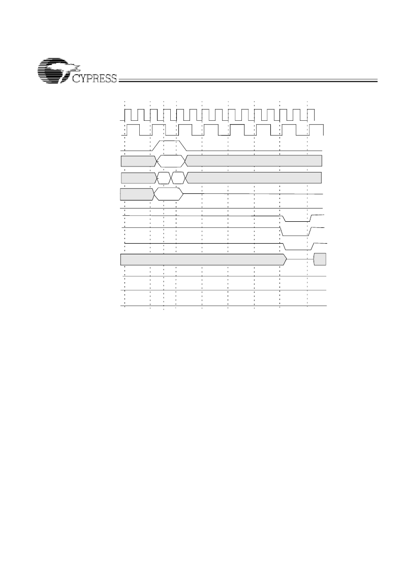
15.5
The following explains the SRAM Read operation accomplished through a table of up to 31 devices using the following param-
eters: TLSZ = 10. The diagram of this table is shown in
Figure 15-5
. The following assumes that SRAM access is being accom-
plished through CYNSE70032 device number 0 and that device number 0 is the selected device.
Figure 15-6
and
Figure 15-7
show the timing diagrams for device number 0 and device number 30, respectively.
Cycle 1A
: The host ASIC applies the Read instruction to CMD[1:0] using CMDV = 1. The DQ bus supplies the address, with
DQ[20:19] set to 10, to select the SRAM address. The host ASIC selects the device for which the ID[4:0] matches the DQ[25:21]
lines. During this cycle, the host ASIC also supplies SADR[21:19] on CMD[8:6].
Cycle 1B
: The host ASIC continues to apply the Read instruction to CMD[1:0] using CMDV = 1. The DQ bus supplies the
address, with DQ[20:19] set to 10, to select the SRAM address.
Cycle 2
: The host ASIC floats DQ[67:0] to a three-state condition.
Cycle 3
: The host ASIC keeps DQ[67:0] in a three-state condition.
Cycle 4
: The selected device starts to drive DQ[67:0].
Cycles 5 to 6
: The selected device continues to drive DQ[67:0].
Cycle 7
: The selected device continues to drive DQ[67:0] and drives an SRAM Read cycle.
Cycle 8
: The selected device drives ACL from Z to LOW.
Cycle 9
: The selected device drives ACK to HIGH.
Cycle 10
: The selected device drives ACK from HIGH to LOW.
At the end of cycle 10, the selected device floats ACL in a three-state condition.
SRAM Read with a Table of up to 31 Devices
cycle
1
CLK2X
CMDV
CMD[1:0]
DQ
Read
Address
OE_L
WE_L
CE_L
SADR
cycle
2
cycle
3
cycle
4
cycle
5
cycle
6
TLSZ = 01, HLAT = 000, LRAM = 1, LDEV = 1.
Figure 15-4. SRAM Read Timing for Device Number 7 in a Block of Eight Devices
PHS_L
CMD[8:2]
A
B
z
0
1
z
z
1
1
SSV
z
SSF
ALE_L
1
z
z
1
z
z
ACK
z
1
相關(guān)PDF資料 |
PDF描述 |
|---|---|
| CYNSE70032-66BGI | Network Search Engine |
| CYNSE70032-83BGC | Network Search Engine |
| CYP15G0403DXB-BGC | Independent Clock Quad HOTLink II⑩ Transceiver |
| CYW15G0403DXB-BGXC | Independent Clock Quad HOTLink II⑩ Transceiver |
| CYW15G0403DXB-BGXI | Independent Clock Quad HOTLink II⑩ Transceiver |
相關(guān)代理商/技術(shù)參數(shù) |
參數(shù)描述 |
|---|---|
| CYNSE70032-66BGI | 制造商:CYPRESS 制造商全稱:Cypress Semiconductor 功能描述:Network Search Engine |
| CYNSE70032-83BGC | 制造商:CYPRESS 制造商全稱:Cypress Semiconductor 功能描述:Network Search Engine |
| CYNSE70064-50BGC | 制造商:Cypress Semiconductor 功能描述: |
| CYNSE70064-83BGC | 制造商:Cypress Semiconductor 功能描述: |
| CYNSE70064A | 制造商:CYPRESS 制造商全稱:Cypress Semiconductor 功能描述:Search Engine |
發(fā)布緊急采購,3分鐘左右您將得到回復。