- 您現(xiàn)在的位置:買賣IC網(wǎng) > PDF目錄378516 > CY8C27666-SPPXC (Cypress Semiconductor Corp.) PSoC⑩ Mixed Signal Array PDF資料下載
參數(shù)資料
| 型號: | CY8C27666-SPPXC |
| 廠商: | Cypress Semiconductor Corp. |
| 英文描述: | PSoC⑩ Mixed Signal Array |
| 中文描述: | ⑩的PSoC混合信號陣列 |
| 文件頁數(shù): | 32/39頁 |
| 文件大?。?/td> | 610K |
| 代理商: | CY8C27666-SPPXC |
第1頁第2頁第3頁第4頁第5頁第6頁第7頁第8頁第9頁第10頁第11頁第12頁第13頁第14頁第15頁第16頁第17頁第18頁第19頁第20頁第21頁第22頁第23頁第24頁第25頁第26頁第27頁第28頁第29頁第30頁第31頁當(dāng)前第32頁第33頁第34頁第35頁第36頁第37頁第38頁第39頁
June 1, 2004
Document No. 38-12019 Rev. *B
32
CY8C27x66 Preliminary Data Sheet
3. Electrical Specifications
3.4.6
AC External Clock Specifications
The following tables list guaranteed maximum and minimum specifications for the voltage and temperature ranges: 4.75V to 5.25V
and -40
°
C
≤
T
A
≤
85
°
C, or 3.0V to 3.6V and -40
°
C
≤
T
A
≤
85
°
C, respectively. Typical parameters apply to 5V and 3.3V at 25
°
C and
are for design guidance only or unless otherwise specified.
3.4.7
AC Programming Specifications
The following table lists guaranteed maximum and minimum specifications for the voltage and temperature ranges: 4.75V to 5.25V
and -40
°
C
≤
T
A
≤
85
°
C, or 3.0V to 3.6V and -40
°
C
≤
T
A
≤
85
°
C, respectively. Typical parameters apply to 5V and 3.3V at 25
°
C and
are for design guidance only or unless otherwise specified.
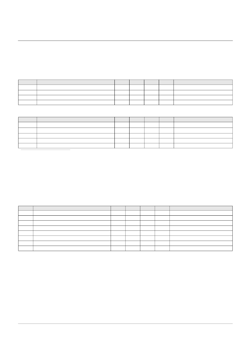
Table 3-23: 5V AC External Clock Specifications
Symbol
Description
Min
Typ
Max
Units
Notes
F
OSCEXT
Frequency
0
–
24.24
MHz
–
High Period
20.6
–
–
ns
–
Low Period
20.6
–
–
ns
μ
s
–
Power Up IMO to Switch
150
–
–
Table 3-24: 3.3V AC External Clock Specifications
Symbol
Description
Min
Typ
Max
Units
Notes
F
OSCEXT
Frequency with CPU Clock divide by 1
a
a. MaximumCPU frequency is 12 MHz at 3.3V. With the CPU clock divider set to 1, the external clock must adhere to the maximumfrequency and duty cycle requirements.
b. If the frequency of the external clock is greater than 12 MHz, the CPU clock divider must be set to 2 or greater. In this case, the CPU clock divider will ensure that the fifty per-
cent duty cycle requirement is met.
0
–
12.12
MHz
F
OSCEXT
Frequency with CPU Clock divide by 2 or greater
b
0
–
24.24
MHz
–
High Period with CPU Clock divide by 1
41.7
–
–
ns
–
Low Period with CPU Clock divide by 1
41.7
–
–
ns
μ
s
–
Power Up IMO to Switch
150
–
–
Table 3-25: AC Programming Specifications
Symbol
T
RSCLK
T
FSCLK
T
SSCLK
T
HSCLK
F
SCLK
T
ERASEB
T
WRITE
T
DSCLK
Description
Min
Typ
Max
Units
ns
Notes
Rise Time of SCLK
1
–
20
Fall Time of SCLK
1
–
20
ns
Data Set up Time to Falling Edge of SCLK
40
–
–
ns
Data Hold Time from Falling Edge of SCLK
40
–
–
ns
Frequency of SCLK
0
–
8
MHz
Flash Erase Time (Block)
–
15
–
ms
Flash Block Write Time
–
30
–
ms
Data Out Delay from Falling Edge of SCLK
–
–
45
ns
相關(guān)PDF資料 |
PDF描述 |
|---|---|
| CY8C27666-SPPXE | PSoC⑩ Mixed Signal Array |
| CY8C27666-SPPXI | PSoC⑩ Mixed Signal Array |
| CY8C27666-SPSXC | PSoC⑩ Mixed Signal Array |
| CY8C27666-SPSXE | PSoC⑩ Mixed Signal Array |
| CY8C27666-SPSXI | PSoC⑩ Mixed Signal Array |
相關(guān)代理商/技術(shù)參數(shù) |
參數(shù)描述 |
|---|---|
| CY8C28000-24PVXI | 制造商:Cypress Semiconductor 功能描述: |
| CY8C28243-24PVXI | 功能描述:可編程片上系統(tǒng) - PSoC PSoC Programmable System-on-Chip RoHS:否 制造商:Cypress Semiconductor 核心:8051 處理器系列:CY8C36 數(shù)據(jù)總線寬度:8 bit 最大時鐘頻率:67 MHz 程序存儲器大小:32 KB 數(shù)據(jù) RAM 大小:4 KB 片上 ADC:Yes 工作電源電壓:0.5 V to 5.5 V 工作溫度范圍:- 40 C to + 85 C 封裝 / 箱體:QFN-68 安裝風(fēng)格:SMD/SMT |
| CY8C28243-24PVXIT | 功能描述:可編程片上系統(tǒng) - PSoC 16 I/O 16K FLASH 1K SRAM RoHS:否 制造商:Cypress Semiconductor 核心:8051 處理器系列:CY8C36 數(shù)據(jù)總線寬度:8 bit 最大時鐘頻率:67 MHz 程序存儲器大小:32 KB 數(shù)據(jù) RAM 大小:4 KB 片上 ADC:Yes 工作電源電壓:0.5 V to 5.5 V 工作溫度范圍:- 40 C to + 85 C 封裝 / 箱體:QFN-68 安裝風(fēng)格:SMD/SMT |
| CY8C28403-24PVXI | 功能描述:可編程片上系統(tǒng) - PSoC PSoC Programmable System-on-Chip RoHS:否 制造商:Cypress Semiconductor 核心:8051 處理器系列:CY8C36 數(shù)據(jù)總線寬度:8 bit 最大時鐘頻率:67 MHz 程序存儲器大小:32 KB 數(shù)據(jù) RAM 大小:4 KB 片上 ADC:Yes 工作電源電壓:0.5 V to 5.5 V 工作溫度范圍:- 40 C to + 85 C 封裝 / 箱體:QFN-68 安裝風(fēng)格:SMD/SMT |
| CY8C28403-24PVXIT | 功能描述:可編程片上系統(tǒng) - PSoC PSoC Programmable System-on-Chip RoHS:否 制造商:Cypress Semiconductor 核心:8051 處理器系列:CY8C36 數(shù)據(jù)總線寬度:8 bit 最大時鐘頻率:67 MHz 程序存儲器大小:32 KB 數(shù)據(jù) RAM 大小:4 KB 片上 ADC:Yes 工作電源電壓:0.5 V to 5.5 V 工作溫度范圍:- 40 C to + 85 C 封裝 / 箱體:QFN-68 安裝風(fēng)格:SMD/SMT |
發(fā)布緊急采購,3分鐘左右您將得到回復(fù)。