- 您現(xiàn)在的位置:買賣IC網(wǎng) > PDF目錄378513 > CY8C21634-24AX (Cypress Semiconductor Corp.) PSoC Mixed-Signal Array PDF資料下載
參數(shù)資料
| 型號: | CY8C21634-24AX |
| 廠商: | Cypress Semiconductor Corp. |
| 英文描述: | PSoC Mixed-Signal Array |
| 中文描述: | PSoC混合信號陣列 |
| 文件頁數(shù): | 25/35頁 |
| 文件大小: | 376K |
| 代理商: | CY8C21634-24AX |
第1頁第2頁第3頁第4頁第5頁第6頁第7頁第8頁第9頁第10頁第11頁第12頁第13頁第14頁第15頁第16頁第17頁第18頁第19頁第20頁第21頁第22頁第23頁第24頁當(dāng)前第25頁第26頁第27頁第28頁第29頁第30頁第31頁第32頁第33頁第34頁第35頁
April 20, 2005
Document No. 38-12025 Rev. *G
25
CY8C21x34 Final Data Sheet
3. Electrical Specifications
3.4.3
AC Operational Amplifier Specifications
The following table lists guaranteed maximum and minimum specifications for the voltage and temperature ranges: 4.75V to 5.25V
and -40
°
C
≤
T
A
≤
85
°
C, 3.0V to 3.6V and -40
°
C
≤
T
A
≤
85
°
C, or 2.4V to 3.0V and -40
°
C
≤
T
A
≤
85
°
C, respectively. Typical parameters
apply to 5V, 3.3V, or 2.7V at 25
°
C and are for design guidance only.
3.4.4
AC Analog Mux Bus Specifications
The following table lists guaranteed maximum and minimum specifications for the voltage and temperature ranges: 4.75V to 5.25V
and -40
°
C
≤
T
A
≤
85
°
C, 3.0V to 3.6V and -40
°
C
≤
T
A
≤
85
°
C, or 2.4V to 3.0V and -40
°
C
≤
T
A
≤
85
°
C, respectively. Typical parameters
apply to 5V, 3.3V, or 2.7V at 25
°
C and are for design guidance only.
3.4.5
AC Digital Block Specifications
The following tables list guaranteed maximum and minimum specifications for the voltage and temperature ranges: 4.75V to 5.25V
and -40
°
C
≤
T
A
≤
85
°
C, 3.0V to 3.6V and -40
°
C
≤
T
A
≤
85
°
C, or 2.4V to 3.0V and -40
°
C
≤
T
A
≤
85
°
C, respectively. Typical parameters
apply to 5V, 3.3V, or 2.7V at 25
°
C and are for design guidance only.
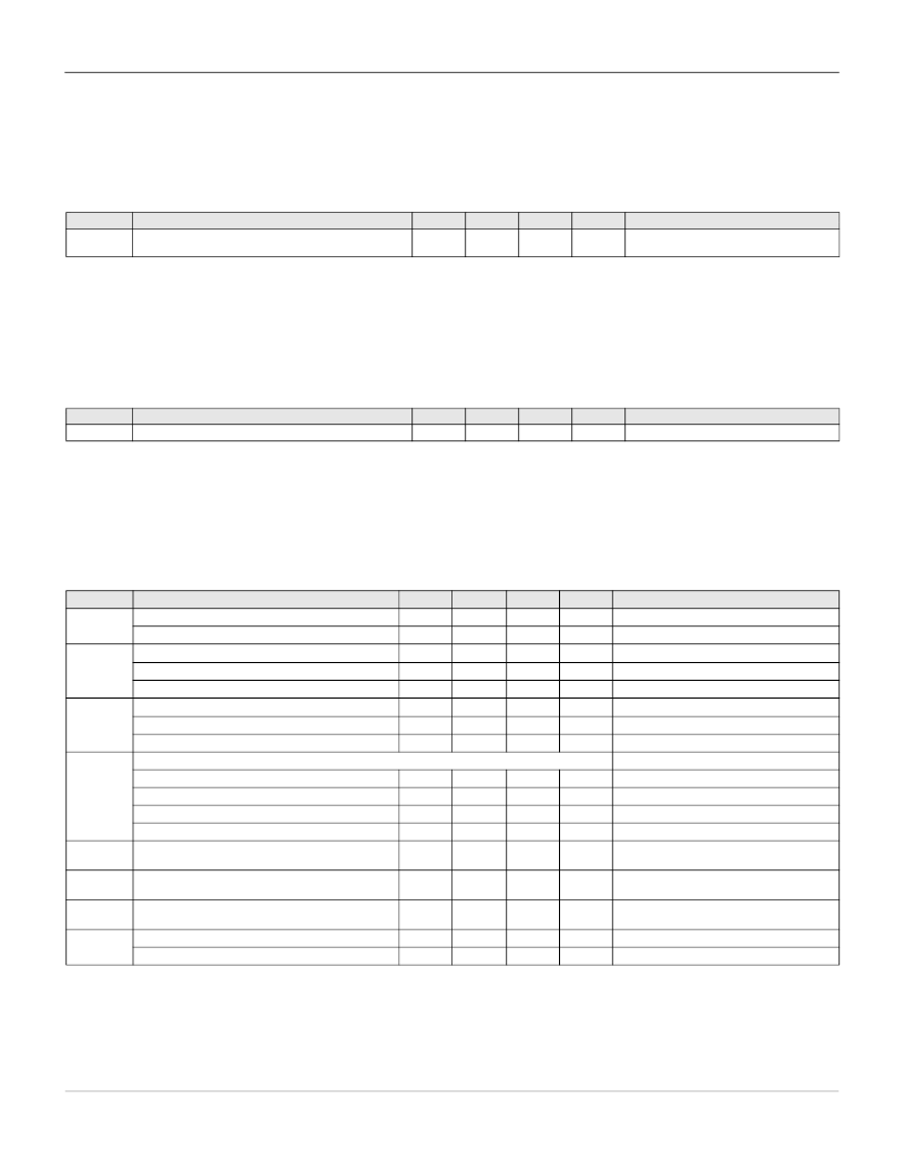
Table 3-18. AC Operational Amplifier Specifications
Symbol
T
COMP
Description
Min
Typ
Max
Units
ns
ns
Notes
Comparator Mode Response Time, 50 mV Overdrive
100
200
Vdd
≥
3.0V.
2.4V < Vcc <
3.0V.
Table 3-19. AC Analog Mux Bus Specifications
Symbol
F
SW
Description
Min
Typ
Max
Units
MHz
Notes
Switch Rate
–
–
3.17
Table 3-20. 5V and 3.3V AC Digital Block Specifications
Function
Description
Min
Typ
Max
Units
Notes
All
Functions
Maximum Block Clocking Frequency (> 4.75V)
49.2
MHz
4.75V < Vdd < 5.25V.
Maximum Block Clocking Frequency (< 4.75V)
24.6
MHz
3.0V < Vdd < 4.75V.
Timer
Capture Pulse Width
50
a
–
–
ns
Maximum Frequency, No Capture
–
–
49.2
MHz
4.75V < Vdd < 5.25V.
Maximum Frequency, With or Without Capture
–
–
24.6
MHz
Counter
Enable Pulse Width
50
–
–
ns
Maximum Frequency, No Enable Input
–
–
49.2
MHz
4.75V < Vdd < 5.25V.
Maximum Frequency, Enable Input
–
–
24.6
MHz
Dead Band
Kill Pulse Width:
Asynchronous Restart Mode
20
–
–
ns
Synchronous Restart Mode
50
–
–
ns
Disable Mode
50
–
–
ns
Maximum Frequency
–
–
49.2
MHz
4.75V < Vdd < 5.25V.
CRCPRS
(PRS Mode)
Maximum Input Clock Frequency
–
–
49.2
MHz
4.75V < Vdd < 5.25V.
CRCPRS
(CRC Mode)
Maximum Input Clock Frequency
–
–
24.6
MHz
SPIM
Maximum Input Clock Frequency
–
–
8.2
MHz
Maximum data rate at 4.1 MHz due to 2 x over
clocking.
SPIS
Maximum Input Clock Frequency
–
–
4.1
MHz
Width of SS_ Negated Between Transmissions
50
–
–
ns
相關(guān)PDF資料 |
PDF描述 |
|---|---|
| CY8C21534 | PSoC Mixed-Signal Array |
| CY8C21234-24LFX | PQ I HIP6W DUET |
| CY8C21434-24LFX | PSoC Mixed-Signal Array |
| CY8C21534-24LFX | PSoC Mixed-Signal Array |
| CY8C21234-24PVX | PSoC Mixed-Signal Array |
相關(guān)代理商/技術(shù)參數(shù) |
參數(shù)描述 |
|---|---|
| CY8C21634-24C | 制造商:CYPRESS 制造商全稱:Cypress Semiconductor 功能描述:PSoC Mixed-Signal Array |
| CY8C21634-24E | 制造商:CYPRESS 制造商全稱:Cypress Semiconductor 功能描述:PSoC Mixed-Signal Array |
| CY8C21634-24I | 制造商:CYPRESS 制造商全稱:Cypress Semiconductor 功能描述:PSoC Mixed-Signal Array |
| CY8C21634-24LFX | 制造商:CYPRESS 制造商全稱:Cypress Semiconductor 功能描述:PSoC Mixed-Signal Array |
| CY8C21634-24LFXI | 功能描述:可編程片上系統(tǒng) - PSoC IC MCU 8K FLASH 512B SRAM RoHS:否 制造商:Cypress Semiconductor 核心:8051 處理器系列:CY8C36 數(shù)據(jù)總線寬度:8 bit 最大時鐘頻率:67 MHz 程序存儲器大小:32 KB 數(shù)據(jù) RAM 大小:4 KB 片上 ADC:Yes 工作電源電壓:0.5 V to 5.5 V 工作溫度范圍:- 40 C to + 85 C 封裝 / 箱體:QFN-68 安裝風(fēng)格:SMD/SMT |
發(fā)布緊急采購,3分鐘左右您將得到回復(fù)。