- 您現(xiàn)在的位置:買賣IC網(wǎng) > PDF目錄379089 > CY7C171A (Cypress Semiconductor Corp.) 4K x 4 Static RAM with Separate I/O(帶獨立的輸入/輸出口的4K x 4靜態(tài) RAM) PDF資料下載
參數(shù)資料
| 型號: | CY7C171A |
| 廠商: | Cypress Semiconductor Corp. |
| 英文描述: | 4K x 4 Static RAM with Separate I/O(帶獨立的輸入/輸出口的4K x 4靜態(tài) RAM) |
| 中文描述: | 4K的× 4靜態(tài)存儲器具有獨立的I / O(帶獨立的輸入/輸出口的4K的靜態(tài)內存× 4) |
| 文件頁數(shù): | 5/9頁 |
| 文件大小: | 165K |
| 代理商: | CY7C171A |
CY7C171A
CY7C172A
5
Switching Characteristics
Over the Operating Range
[2,5]
7C171A-15
7C172A-15
Min.
7C171A-20
7C172A-20
Min.
7C171A-25
7C172A-25
Min.
7C171A-35
7C172A-35
Min.
7C171A-45
7C172A-45
Min.
Parameter
Description
Max.
Max.
Max.
Max.
Max.
Unit
READ CYCLE
t
RC
t
AA
t
OHA
t
ACE
t
LZCE
t
HZCE
t
PU
t
PD
t
RCS
t
RCH
WRITE CYCLE
[8]
Read Cycle Time
15
20
25
35
45
ns
Address to Data Valid
15
20
25
35
45
ns
Output Hold from Address Change
5
5
5
5
5
ns
CE LOW to Data Valid
CE LOW to LOW Z
[6]
CE HIGH to HIGH Z
[6, 7]
15
20
25
35
45
ns
5
5
5
5
5
ns
8
8
10
15
15
ns
CE LOW to Power Up
0
0
0
0
0
ns
CE HIGH to Power Down
15
20
20
20
25
ns
Read Command Set-Up
0
0
0
0
0
ns
Read Command Hold
0
0
0
0
0
ns
t
WC
t
SCE
t
AW
t
HA
t
SA
t
PWE
t
SD
t
HD
t
LZWE
t
HZWE
t
AWE
t
ADV
Write Cycle Time
15
20
20
25
40
ns
CE LOW to Write End
12
15
20
25
30
ns
Address Set-Up to Write End
12
15
20
25
30
ns
Address Hold from Write End
0
0
0
0
0
ns
Address Set-Up to Write Start
0
0
0
0
0
ns
WE Pulse Width
12
15
15
20
20
ns
Data Set-Up to Write End
10
10
10
15
15
ns
Data Hold from Write End
WE HIGH to Low Z
[6]
(7C172A)
WE LOW to High Z
[6,7]
(7C172A)
0
0
0
0
0
ns
5
5
5
5
5
ns
7
7
7
10
15
ns
WE LOW to Data Valid (7C171A)
15
20
25
30
35
ns
Data Valid to Output Valid
(7C171A)
15
20
25
30
35
ns
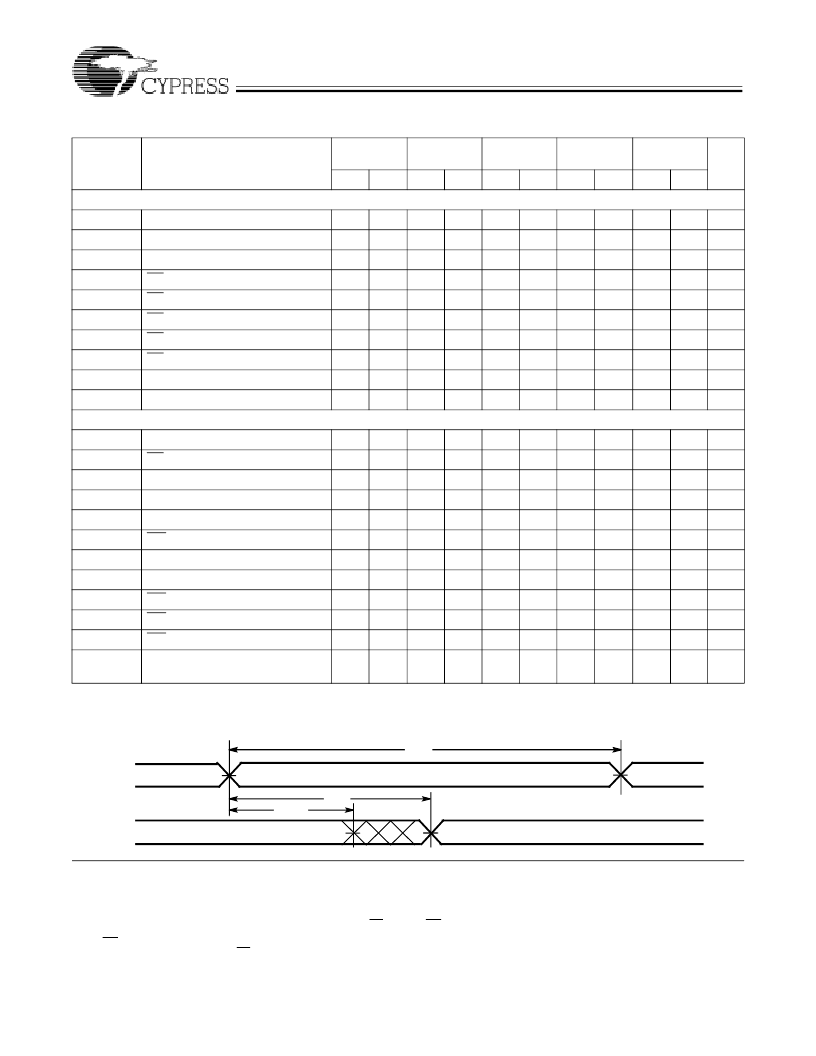
Switching Waveforms
Read Cycle No. 1
[9,10]
Notes:
5.
Test conditions assume signal transition times of 5 ns or less, timing reference levels of 1.5V, input pulse levels of 0 to 3.0V and output loading of the specified
I
/I
and 30-pF load capacitance.
At any given temperature and voltage condition, t
is less than t
for any given device.
t
and t
are tested with C
= 5pF as in part (b) of AC Test Loads. Transition is measured
±
500 mV from steady state voltage.
The internal write time of the memory is defined by the overlap of CE LOW and WE LOW. Both signals must be LOW to initiate a write and either signal can
terminate a write by going HIGH. The data input setup and hold timing should be referenced to the rising edge of the signal that terminates the write.
WE is HIGH for read cycle.
10. Device is continuously selected, CE = V
IL
.
6.
7.
8.
9.
PREVIOUS DATA VALID
DATA VALID
t
RC
t
AA
t
OHA
ADDRESS
DATA OUT
C171A–5
相關PDF資料 |
PDF描述 |
|---|---|
| CY7C172A | 4K x 4 Static RAM with Separate I/O(帶獨立的輸入/輸出口的4K x 4靜態(tài) RAM) |
| CY7C185A | 8K x 8 Static RAM(8Kx8靜態(tài) RAM) |
| CY7C1916BV18 | 18-Mbit DDR-II SRAM 2-Word Burst Architecture(2字Burst結構,18-Mbit DDR-II SRAM) |
| CY7C1320BV18 | 18-Mbit DDR-II SRAM 2-Word Burst Architecture(2字Burst結構,18-Mbit DDR-II SRAM) |
| CY7C1316BV18 | 18-Mbit DDR-II SRAM 2-Word Burst Architecture(2字Burst結構,18-Mbit DDR-II SRAM) |
相關代理商/技術參數(shù) |
參數(shù)描述 |
|---|---|
| CY7C172A-15VC | 制造商:Cypress Semiconductor 功能描述: |
| CY7C172A-15VCT | 制造商:Cypress Semiconductor 功能描述: |
| CY7C172A45DMB | 制造商:CYPRESS 功能描述:New |
| CY7C172A-45DMB | 制造商:Rochester Electronics LLC 功能描述:- Bulk |
| CY7C172A-45VC | 制造商:Rochester Electronics LLC 功能描述:- Bulk 制造商:Cypress Semiconductor 功能描述: |
發(fā)布緊急采購,3分鐘左右您將得到回復。