- 您現(xiàn)在的位置:買賣IC網(wǎng) > PDF目錄379089 > CY7C1527V18-300BZXC (CYPRESS SEMICONDUCTOR CORP) 72-Mbit DDR-II SRAM 2-Word Burst Architecture PDF資料下載
參數(shù)資料
| 型號(hào): | CY7C1527V18-300BZXC |
| 廠商: | CYPRESS SEMICONDUCTOR CORP |
| 元件分類: | DRAM |
| 英文描述: | 72-Mbit DDR-II SRAM 2-Word Burst Architecture |
| 中文描述: | 8M X 9 DDR SRAM, 0.45 ns, PBGA165 |
| 封裝: | 15 X 17 MM, 1.40 MM HEIGHT, LEAD FREE, MO-216, FBGA-165 |
| 文件頁(yè)數(shù): | 9/28頁(yè) |
| 文件大小: | 457K |
| 代理商: | CY7C1527V18-300BZXC |
第1頁(yè)第2頁(yè)第3頁(yè)第4頁(yè)第5頁(yè)第6頁(yè)第7頁(yè)第8頁(yè)當(dāng)前第9頁(yè)第10頁(yè)第11頁(yè)第12頁(yè)第13頁(yè)第14頁(yè)第15頁(yè)第16頁(yè)第17頁(yè)第18頁(yè)第19頁(yè)第20頁(yè)第21頁(yè)第22頁(yè)第23頁(yè)第24頁(yè)第25頁(yè)第26頁(yè)第27頁(yè)第28頁(yè)
CY7C1516V18
CY7C1527V18
CY7C1518V18
CY7C1520V18
Document #: 38-05563 Rev. *D
Page 9 of 28
Programmable Impedance
An external resistor, RQ, must be connected between the ZQ
pin on the SRAM and V
SS
to allow the SRAM to adjust its
output driver impedance. The value of RQ must be 5x the
value of the intended line impedance driven by the SRAM, The
allowable range of RQ to guarantee impedance matching with
a tolerance of ±15% is between 175
and 350
,
with
V
DDQ
= 1.5V. The output impedance is adjusted every 1024
cycles upon power-up to account for drifts in supply voltage
and temperature.
Echo Clocks
Echo clocks are provided on the DDR-II to simplify data
capture on high-speed systems. Two echo clocks are
generated by the DDR-II. CQ is referenced with respect to C
and CQ is referenced with respect to C. These are
free-running clocks and are synchronized to the output clock
of the DDR-II. In the single clock mode, CQ is generated with
respect to K and CQ is generated with respect to K. The
timings for the echo clocks are shown in the AC Timing table.
DLL
These chips utilize a Delay Lock Loop (DLL) that is designed
to function between 80 MHz and the specified maximum clock
frequency. During power-up, when the DOFF is tied HIGH, the
DLL gets locked after 1024 cycles of stable clock. The DLL can
also be reset by slowing or stopping the input clock K and K
for a minimum of 30 ns. However, it is not necessary for the
DLL to be specifically reset in order to lock the DLL to the
desired frequency. The DLL will automatically lock 1024 clock
cycles after a stable clock is presented.the DLL may be
disabled by applying ground to the DOFF pin. For information
refer to the application note “DLL Considerations in
QDRII/DDRII/QDRII+/DDRII+”.
Notes:
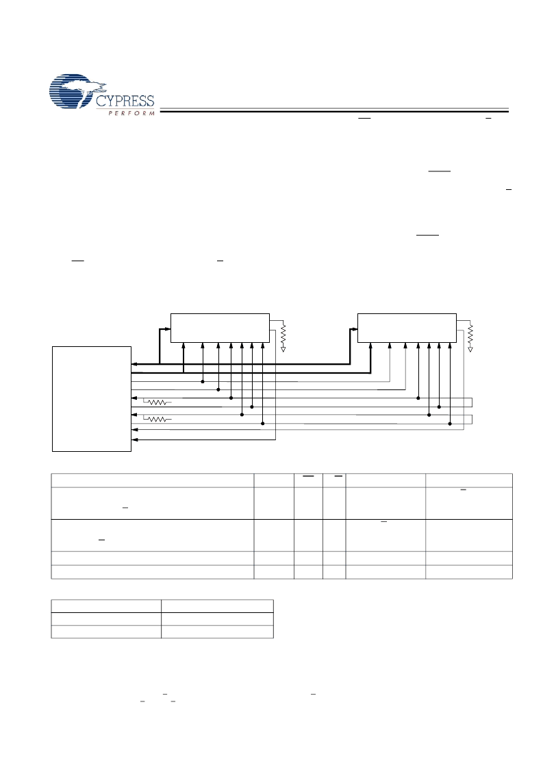
2. The above application shows two DDR-II used.
3. X = “Don’t Care,” H = Logic HIGH, L = Logic LOW,
↑
represents rising edge.
4. Device will power-up deselected and the outputs in a tri-state condition.
5. On CY7C1518V18 and CY7C1520V18, “A1” represents address location latched by the devices when transaction was initiated and A2 represents the addresses
sequence in the burst. On CY7C1516V18, “A1” represents A +‘0’ and A2 represents A +‘1.’
6. “t” represents the cycle at which a Read/Write operation is started. t+1 and t + 2 are the first and second clock cycles succeeding the “t” clock cycle.
7. Data inputs are registered at K and K rising edges. Data outputs are delivered on C and C rising edges, except when in single clock mode.
8. It is recommended that K = K and C = C = HIGH when clock is stopped. This is not essential, but permits most rapid restart by overcoming transmission line
charging symmetrically.
Application Example
[2]
Truth Table
[3, 4, 5, 6, 7, 8]
Operation
K
LD
L
R/W
L
DQ
DQ
Write Cycle:
Load address; wait one cycle; input write data on
consecutive K and K rising edges.
Read Cycle:
Load address; wait one and a half cycle; read data on
consecutive C and C rising edges.
NOP: No Operation
Standby: Clock Stopped
L-H
D(A1) at K(t + 1)
↑
D(A2) at K(t + 1)
↑
L-H
L
H
Q(A1) at C(t + 1)
↑
Q(A2) at C(t + 2)
↑
L-H
H
X
X
X
Previous State
High-Z
Previous State
Stopped
LD#
Vterm = 0.75V
Vterm = 0.75V
C C#
R/W#
ZQ
CQ/CQ#
K#
DQ
A
LD#
C C#
R/W#
ZQ
CQ/CQ#
K#
DQ
A
BUS
MASTER
(CPU
or
ASIC)
SRAM#1
SRAM#2
DQ
Addresses
Cycle Start#
R/W#
Return CLK
Source CLK
Return CLK#
Source CLK#
Echo Clock1/Echo Clock#1
Echo Clock2/Echo Clock#2
R = 50
ohms
R = 250
ohms
R
= 250ohms
Burst Address Table
(CY7C1518V18, CY7C1520V18)
First Address (External)
X..X0
X..X1
Second Address (Internal)
X..X1
X..X0
[+] Feedback
相關(guān)PDF資料 |
PDF描述 |
|---|---|
| CY7C1527V18-300BZXI | 72-Mbit DDR-II SRAM 2-Word Burst Architecture |
| CY7C171A | 4K x 4 Static RAM with Separate I/O(帶獨(dú)立的輸入/輸出口的4K x 4靜態(tài) RAM) |
| CY7C172A | 4K x 4 Static RAM with Separate I/O(帶獨(dú)立的輸入/輸出口的4K x 4靜態(tài) RAM) |
| CY7C185A | 8K x 8 Static RAM(8Kx8靜態(tài) RAM) |
| CY7C1916BV18 | 18-Mbit DDR-II SRAM 2-Word Burst Architecture(2字Burst結(jié)構(gòu),18-Mbit DDR-II SRAM) |
相關(guān)代理商/技術(shù)參數(shù) |
參數(shù)描述 |
|---|---|
| CY7C1543KV18-400BZC | 功能描述:靜態(tài)隨機(jī)存取存儲(chǔ)器 72MB (4Mx18) 1.8v 400MHz QDR II 靜態(tài)隨機(jī)存取存儲(chǔ)器 RoHS:否 制造商:Cypress Semiconductor 存儲(chǔ)容量:16 Mbit 組織:1 M x 16 訪問(wèn)時(shí)間:55 ns 電源電壓-最大:3.6 V 電源電壓-最小:2.2 V 最大工作電流:22 uA 最大工作溫度:+ 85 C 最小工作溫度:- 40 C 安裝風(fēng)格:SMD/SMT 封裝 / 箱體:TSOP-48 封裝:Tray |
| CY7C1543KV18-400BZI | 功能描述:靜態(tài)隨機(jī)存取存儲(chǔ)器 72MB (4Mx18) 1.8v 400MHz QDR II 靜態(tài)隨機(jī)存取存儲(chǔ)器 RoHS:否 制造商:Cypress Semiconductor 存儲(chǔ)容量:16 Mbit 組織:1 M x 16 訪問(wèn)時(shí)間:55 ns 電源電壓-最大:3.6 V 電源電壓-最小:2.2 V 最大工作電流:22 uA 最大工作溫度:+ 85 C 最小工作溫度:- 40 C 安裝風(fēng)格:SMD/SMT 封裝 / 箱體:TSOP-48 封裝:Tray |
| CY7C1543KV18-450BZC | 功能描述:靜態(tài)隨機(jī)存取存儲(chǔ)器 4Mb x 18 450 MHz RoHS:否 制造商:Cypress Semiconductor 存儲(chǔ)容量:16 Mbit 組織:1 M x 16 訪問(wèn)時(shí)間:55 ns 電源電壓-最大:3.6 V 電源電壓-最小:2.2 V 最大工作電流:22 uA 最大工作溫度:+ 85 C 最小工作溫度:- 40 C 安裝風(fēng)格:SMD/SMT 封裝 / 箱體:TSOP-48 封裝:Tray |
| CY7C1543KV18-450BZI | 功能描述:靜態(tài)隨機(jī)存取存儲(chǔ)器 72MB (8Mx9) 1.8v 450MHz QDR II 靜態(tài)隨機(jī)存取存儲(chǔ)器 RoHS:否 制造商:Cypress Semiconductor 存儲(chǔ)容量:16 Mbit 組織:1 M x 16 訪問(wèn)時(shí)間:55 ns 電源電壓-最大:3.6 V 電源電壓-最小:2.2 V 最大工作電流:22 uA 最大工作溫度:+ 85 C 最小工作溫度:- 40 C 安裝風(fēng)格:SMD/SMT 封裝 / 箱體:TSOP-48 封裝:Tray |
| CY7C1543V18-333BZC | 功能描述:靜態(tài)隨機(jī)存取存儲(chǔ)器 72M Q2+ B4 (2.0) RoHS:否 制造商:Cypress Semiconductor 存儲(chǔ)容量:16 Mbit 組織:1 M x 16 訪問(wèn)時(shí)間:55 ns 電源電壓-最大:3.6 V 電源電壓-最小:2.2 V 最大工作電流:22 uA 最大工作溫度:+ 85 C 最小工作溫度:- 40 C 安裝風(fēng)格:SMD/SMT 封裝 / 箱體:TSOP-48 封裝:Tray |
發(fā)布緊急采購(gòu),3分鐘左右您將得到回復(fù)。