- 您現(xiàn)在的位置:買賣IC網(wǎng) > PDF目錄379058 > CY7C1245V18-300BZI (CYPRESS SEMICONDUCTOR CORP) 36-Mbit QDR⑩-II+ SRAM 4-Word Burst Architecture (2.0 Cycle Read Latency) PDF資料下載
參數(shù)資料
| 型號(hào): | CY7C1245V18-300BZI |
| 廠商: | CYPRESS SEMICONDUCTOR CORP |
| 元件分類: | DRAM |
| 英文描述: | 36-Mbit QDR⑩-II+ SRAM 4-Word Burst Architecture (2.0 Cycle Read Latency) |
| 中文描述: | 1M X 36 QDR SRAM, 0.45 ns, PBGA165 |
| 封裝: | 15 X 17 MM, 1.40 MM HEIGHT, MO-216, FBGA-165 |
| 文件頁數(shù): | 12/28頁 |
| 文件大?。?/td> | 1042K |
| 代理商: | CY7C1245V18-300BZI |
第1頁第2頁第3頁第4頁第5頁第6頁第7頁第8頁第9頁第10頁第11頁當(dāng)前第12頁第13頁第14頁第15頁第16頁第17頁第18頁第19頁第20頁第21頁第22頁第23頁第24頁第25頁第26頁第27頁第28頁
CY7C1241V18
CY7C1256V18
CY7C1243V18
CY7C1245V18
Document Number: 001-06365 Rev. *C
Page 12 of 28
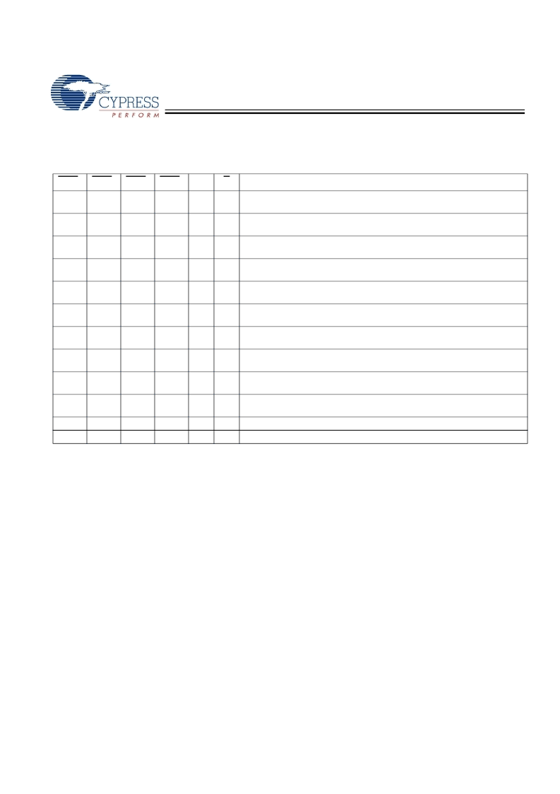
Write Cycle Descriptions
The write cycle description table for CY7C1245V18 follows.
[2, 10]
BWS
0
L
BWS
1
L
BWS
2
L
BWS
3
L
K
K
Comments
L–H
–
During the data portion of a write sequence, all four bytes (D
[35:0]
) are written
into the device.
L–H During the data portion of a write sequence, all four bytes (D
[35:0]
) are written
into the device.
–
During the data portion of a write sequence, only the lower byte (D
[8:0]
) is
written into the device. D
[35:9]
remains unaltered.
L–H During the data portion of a write sequence, only the lower byte (D
[8:0]
) is
written into the device. D
[35:9]
remains unaltered.
–
During the data portion of a write sequence, only the byte (D
[17:9]
) is written
into the device. D
[8:0]
and D
[35:18]
remain unaltered.
L–H During the data portion of a write sequence, only the byte (D
[17:9]
) is written
into the device. D
[8:0]
and D
[35:18]
remain unaltered.
–
During the data portion of a write sequence, only the byte (D
[26:18]
) is written
into the device. D
[17:0]
and D
[35:27]
remain unaltered.
L–H During the data portion of a write sequence, only the byte (D
[26:18]
) is written
into the device. D
[17:0]
and D
[35:27]
remain unaltered.
–
During the data portion of a write sequence, only the byte (D
[35:27]
) is written
into the device. D
[26:0]
remains unaltered.
L–H During the data portion of a write sequence, only the byte (D
[35:27]
) is written
into the device. D
[26:0]
remains unaltered.
–
No data is written into the device during this portion of a write operation.
L–H No data is written into the device during this portion of a write operation.
L
L
L
L
–
L
H
H
H
L–H
L
H
H
–
H
L
H
H
L–H
H
L
H
H
–
H
H
L
H
L–H
H
H
L
H
–
H
H
H
L
L–H
H
H
H
L
–
H
H
H
H
H
H
H
H
L–H
–
[+] Feedback
相關(guān)PDF資料 |
PDF描述 |
|---|---|
| CY7C1245V18-300BZXC | 36-Mbit QDR⑩-II+ SRAM 4-Word Burst Architecture (2.0 Cycle Read Latency) |
| CY7C1245V18-300BZXI | 36-Mbit QDR⑩-II+ SRAM 4-Word Burst Architecture (2.0 Cycle Read Latency) |
| CY7C1256V18 | 36-Mbit QDR⑩-II+ SRAM 4-Word Burst Architecture (2.0 Cycle Read Latency) |
| CY7C1256V18-300BZC | 36-Mbit QDR⑩-II+ SRAM 4-Word Burst Architecture (2.0 Cycle Read Latency) |
| CY7C1256V18-300BZI | 36-Mbit QDR⑩-II+ SRAM 4-Word Burst Architecture (2.0 Cycle Read Latency) |
相關(guān)代理商/技術(shù)參數(shù) |
參數(shù)描述 |
|---|---|
| CY7C1245V18-375BZC | 制造商:Cypress Semiconductor 功能描述: |
| CY7C1245XC | 制造商:Cypress Semiconductor 功能描述: |
| CY7C12481KV18-400BZC | 功能描述:靜態(tài)隨機(jī)存取存儲(chǔ)器 2M X 18 400MHz DDR II+ 靜態(tài)隨機(jī)存取存儲(chǔ)器 RoHS:否 制造商:Cypress Semiconductor 存儲(chǔ)容量:16 Mbit 組織:1 M x 16 訪問時(shí)間:55 ns 電源電壓-最大:3.6 V 電源電壓-最小:2.2 V 最大工作電流:22 uA 最大工作溫度:+ 85 C 最小工作溫度:- 40 C 安裝風(fēng)格:SMD/SMT 封裝 / 箱體:TSOP-48 封裝:Tray |
| CY7C12481KV18-400BZXC | 功能描述:IC SRAM 36MBIT 400MHZ 165-FPBGA RoHS:是 類別:集成電路 (IC) >> 存儲(chǔ)器 系列:- 標(biāo)準(zhǔn)包裝:150 系列:- 格式 - 存儲(chǔ)器:EEPROMs - 串行 存儲(chǔ)器類型:EEPROM 存儲(chǔ)容量:4K (2 x 256 x 8) 速度:400kHz 接口:I²C,2 線串口 電源電壓:2.5 V ~ 5.5 V 工作溫度:-40°C ~ 85°C 封裝/外殼:8-VFDFN 裸露焊盤 供應(yīng)商設(shè)備封裝:8-DFN(2x3) 包裝:管件 產(chǎn)品目錄頁面:1445 (CN2011-ZH PDF) |
| CY7C1248KV18-400BZC | 功能描述:靜態(tài)隨機(jī)存取存儲(chǔ)器 36MB (2Mx18) 1.8v 400MHz DDR II 靜態(tài)隨機(jī)存取存儲(chǔ)器 RoHS:否 制造商:Cypress Semiconductor 存儲(chǔ)容量:16 Mbit 組織:1 M x 16 訪問時(shí)間:55 ns 電源電壓-最大:3.6 V 電源電壓-最小:2.2 V 最大工作電流:22 uA 最大工作溫度:+ 85 C 最小工作溫度:- 40 C 安裝風(fēng)格:SMD/SMT 封裝 / 箱體:TSOP-48 封裝:Tray |
發(fā)布緊急采購,3分鐘左右您將得到回復(fù)。