- 您現(xiàn)在的位置:買賣IC網 > PDF目錄378497 > CY7C1165V18 (Cypress Semiconductor Corp.) 18-Mbit QDR⑩-II+ SRAM 4-Word Burst Architecture (2.5 Cycle Read Latency) PDF資料下載
參數(shù)資料
| 型號: | CY7C1165V18 |
| 廠商: | Cypress Semiconductor Corp. |
| 英文描述: | 18-Mbit QDR⑩-II+ SRAM 4-Word Burst Architecture (2.5 Cycle Read Latency) |
| 中文描述: | 18兆位的國防評估報告⑩- II SRAM的4字突發(fā)架構(2.5周期讀寫延遲) |
| 文件頁數(shù): | 12/29頁 |
| 文件大小: | 956K |
| 代理商: | CY7C1165V18 |
第1頁第2頁第3頁第4頁第5頁第6頁第7頁第8頁第9頁第10頁第11頁當前第12頁第13頁第14頁第15頁第16頁第17頁第18頁第19頁第20頁第21頁第22頁第23頁第24頁第25頁第26頁第27頁第28頁第29頁
CY7C1161V18
CY7C1176V18
CY7C1163V18
CY7C1165V18
Document Number: 001-06582 Rev. *C
Page 12 of 29
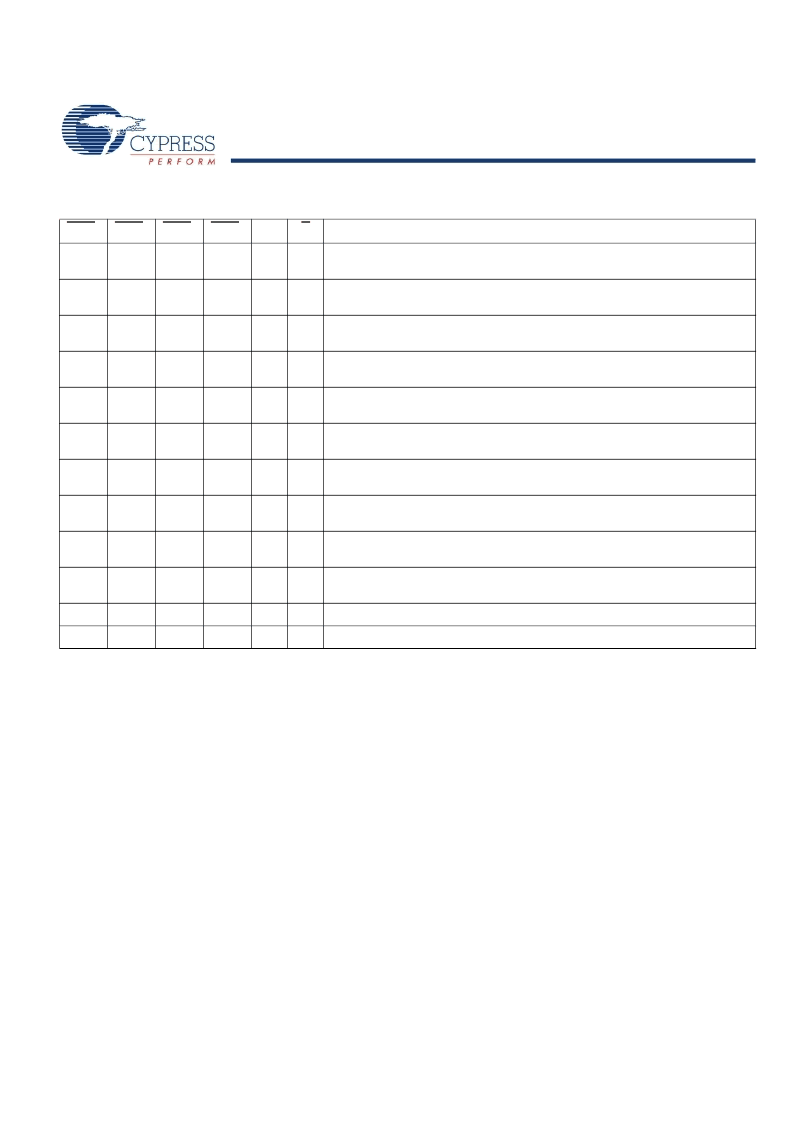
The write cycle descriptions of CY7C1165V18 follows.
[3, 11]
BWS
0
BWS
1
BWS
2
BWS
3
K
K
Comments
L
L
L
L
L–H
–
During the data portion of a write sequence, all four bytes (D
[35:0]
) are written into
the device.
L
L
L
L
–
L–H During the data portion of a write sequence, all four bytes (D
[35:0]
) are written into
the device.
L
H
H
H
L–H
–
During thedata portion of a write sequence, only the lower byte (D
[8:0]
) is written
into the device. D
[35:9]
remains unaltered.
L
H
H
H
–
L–H During the data portion of a write sequence, only the lower byte (D
[8:0]
) is written
into the device. D
[35:9]
remains unaltered.
H
L
H
H
L–H
–
During the data portion of a write sequence, only the byte (D
[17:9]
) is written into
the device. D
[8:0]
and D
[35:18]
remains unaltered.
H
L
H
H
–
L–H During the data portion of a write sequence, only the byte (D
[17:9]
) is written into
the device. D
[8:0]
and D
[35:18]
remains unaltered.
H
H
L
H
L–H
–
During the data portion of a write sequence, only the byte (D
[26:18]
) is written into
the device. D
[17:0]
and D
[35:27]
remains unaltered.
H
H
L
H
–
L–H During the data portion of a write sequence, only the byte (D
[26:18]
) is written into
the device. D
[17:0]
and D
[35:27]
remains unaltered.
H
H
H
L
L–H
–
During the data portion of a write sequence, only the byte (D
[35:27]
) is written into
the device. D
[26:0]
remains unaltered.
H
H
H
L
–
L–H During the data portion of a write sequence, only the byte (D
[35:27]
) is written into
the device. D
[26:0]
remains unaltered.
H
H
H
H
L–H
–
No data is written into the device during this portion of a write operation.
H
H
H
H
–
L–H No data is written into the device during this portion of a write operation.
[+] Feedback
相關PDF資料 |
PDF描述 |
|---|---|
| CY7C1165V18-300BZC | 18-Mbit QDR⑩-II+ SRAM 4-Word Burst Architecture (2.5 Cycle Read Latency) |
| CY7C1165V18-300BZI | 18-Mbit QDR⑩-II+ SRAM 4-Word Burst Architecture (2.5 Cycle Read Latency) |
| CY7C1165V18-300BZXC | 18-Mbit QDR⑩-II+ SRAM 4-Word Burst Architecture (2.5 Cycle Read Latency) |
| CY7C1165V18-300BZXI | 18-Mbit QDR⑩-II+ SRAM 4-Word Burst Architecture (2.5 Cycle Read Latency) |
| CY7C1165V18-333BZC | 18-Mbit QDR⑩-II+ SRAM 4-Word Burst Architecture (2.5 Cycle Read Latency) |
相關代理商/技術參數(shù) |
參數(shù)描述 |
|---|---|
| CY7C1165V18-300BZXC | 制造商:Cypress Semiconductor 功能描述: |
| CY7C1165V18-400BZXC | 功能描述:靜態(tài)隨機存取存儲器 18M Q+, B4 2.5 LATENCY RoHS:否 制造商:Cypress Semiconductor 存儲容量:16 Mbit 組織:1 M x 16 訪問時間:55 ns 電源電壓-最大:3.6 V 電源電壓-最小:2.2 V 最大工作電流:22 uA 最大工作溫度:+ 85 C 最小工作溫度:- 40 C 安裝風格:SMD/SMT 封裝 / 箱體:TSOP-48 封裝:Tray |
| CY7C1165XC | 制造商:Cypress Semiconductor 功能描述: |
| CY7C11681KV18-400BZC | 功能描述:靜態(tài)隨機存取存儲器 1Mb x 18 400 MHz Sync 靜態(tài)隨機存取存儲器 RoHS:否 制造商:Cypress Semiconductor 存儲容量:16 Mbit 組織:1 M x 16 訪問時間:55 ns 電源電壓-最大:3.6 V 電源電壓-最小:2.2 V 最大工作電流:22 uA 最大工作溫度:+ 85 C 最小工作溫度:- 40 C 安裝風格:SMD/SMT 封裝 / 箱體:TSOP-48 封裝:Tray |
| CY7C11681KV18-400BZXC | 功能描述:靜態(tài)隨機存取存儲器 1Mb x 18 400 MHz Sync 靜態(tài)隨機存取存儲器 RoHS:否 制造商:Cypress Semiconductor 存儲容量:16 Mbit 組織:1 M x 16 訪問時間:55 ns 電源電壓-最大:3.6 V 電源電壓-最小:2.2 V 最大工作電流:22 uA 最大工作溫度:+ 85 C 最小工作溫度:- 40 C 安裝風格:SMD/SMT 封裝 / 箱體:TSOP-48 封裝:Tray |
發(fā)布緊急采購,3分鐘左右您將得到回復。