- 您現(xiàn)在的位置:買賣IC網(wǎng) > PDF目錄170346 > CY39050V208-125NTXC (CYPRESS SEMICONDUCTOR CORP) LOADABLE PLD, 10 ns, PQFP208 PDF資料下載
參數(shù)資料
| 型號(hào): | CY39050V208-125NTXC |
| 廠商: | CYPRESS SEMICONDUCTOR CORP |
| 元件分類: | PLD |
| 英文描述: | LOADABLE PLD, 10 ns, PQFP208 |
| 封裝: | 28 X 28 MM, 0.50 MM PITCH, LEAD FREE, PLASTIC, EQFP-208 |
| 文件頁數(shù): | 23/86頁 |
| 文件大?。?/td> | 2802K |
| 代理商: | CY39050V208-125NTXC |
第1頁第2頁第3頁第4頁第5頁第6頁第7頁第8頁第9頁第10頁第11頁第12頁第13頁第14頁第15頁第16頁第17頁第18頁第19頁第20頁第21頁第22頁當(dāng)前第23頁第24頁第25頁第26頁第27頁第28頁第29頁第30頁第31頁第32頁第33頁第34頁第35頁第36頁第37頁第38頁第39頁第40頁第41頁第42頁第43頁第44頁第45頁第46頁第47頁第48頁第49頁第50頁第51頁第52頁第53頁第54頁第55頁第56頁第57頁第58頁第59頁第60頁第61頁第62頁第63頁第64頁第65頁第66頁第67頁第68頁第69頁第70頁第71頁第72頁第73頁第74頁第75頁第76頁第77頁第78頁第79頁第80頁第81頁第82頁第83頁第84頁第85頁第86頁
Delta39K ISR
CPLD Family
Document #: 38-03039 Rev. *I
Page 3 of 86
General Description
The Delta39K family, based on a 0.18-mm, six-layer metal
CMOS logic process, offers a wide range of high-density
solutions at unparalleled system performance. The Delta39K
family is designed to combine the high speed, predictable
timing, and ease of use of CPLDs with the high densities and
low power of FPGAs. With devices ranging from 30,000 to
200,000 usable gates, the family features devices ten times
the size of previously available CPLDs. Even at these large
densities, the Delta39K family is fast enough to implement a
fully synthesizable 64-bit, 66-MHz PCI core.
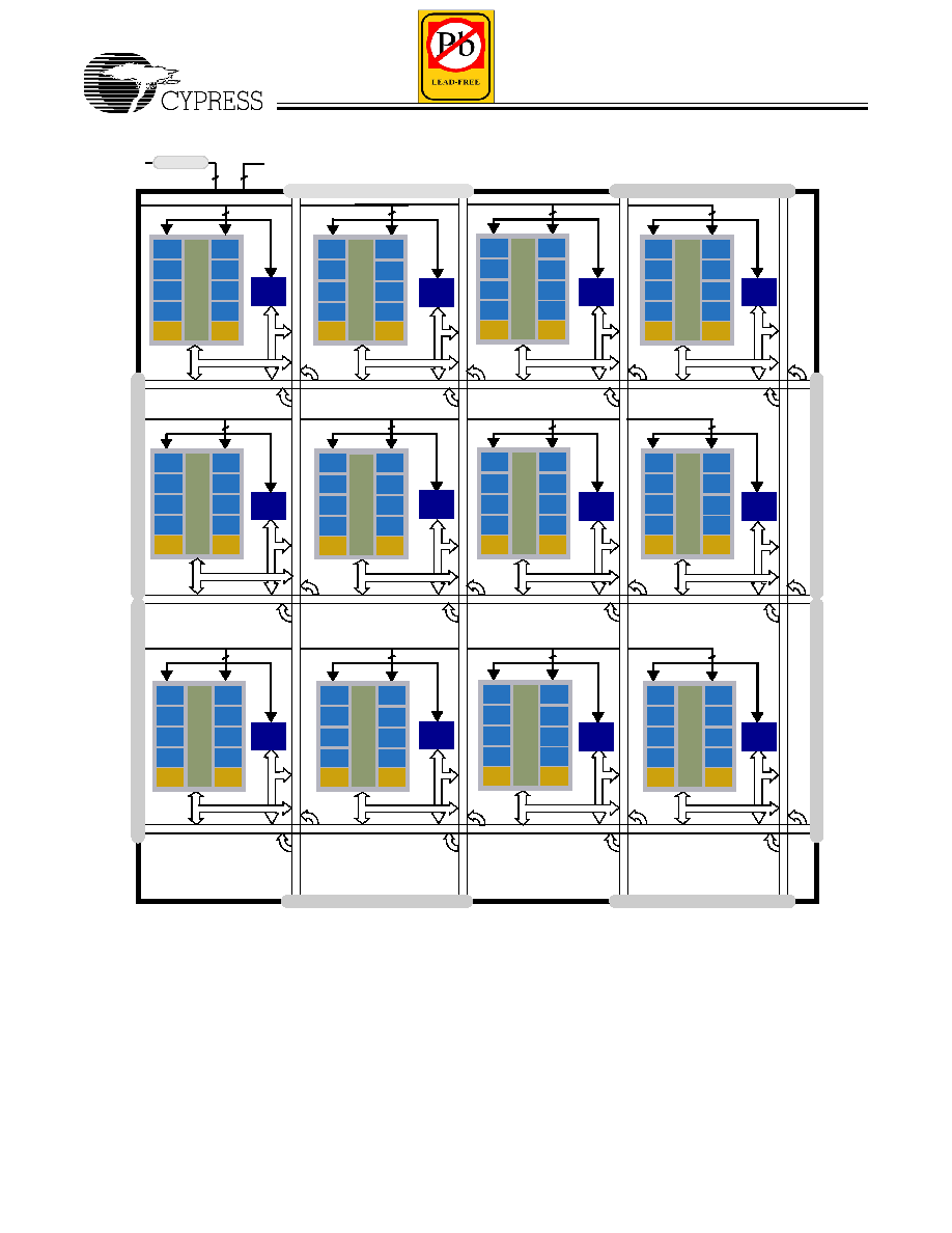
The architecture is based on Logic Block Clusters (LBC) that
are connected by Horizontal and Vertical (H and V) routing
channels. Each LBC features eight individual Logic Blocks
(LB) and two cluster memory blocks. Adjacent to each LBC is
a channel memory block, which can be accessed directly from
the I/O pins. Both types of memory blocks are highly config-
urable and can be cascaded in width and depth. See Figure 1
for a block diagram of the Delta39K architecture.
All the members of the Delta39K family have Cypress’s highly
regarded In-System Reprogrammability (ISR) feature, which
simplifies both design and manufacturing flows, thereby
reducing costs. The ISR feature provides the ability to recon-
4
GCLK[3:0]
4
Channel
RAM
4
GCLK[3:0]
4
GCLK[3:0]
4
GCLK[3:0] PLL and Clock MUX
GCTL[3:0]
I/O Bank 6
I/O Bank 7
I/O Bank 3
I/O Bank 2
I/O
Ba
nk
4
I/O
Bank
5
I/O
Ba
nk
1
I/O
Bank
0
LB 4
LB 3
LB 0
Cluster
RAM
LB 5
LB 6
LB 7
LB 2
LB 1
PIM
Cluster
RAM
Channel
RAM
Channel
RAM
Channel
RAM
Channel
RAM
Channel
RAM
Channel
RAM
Channel
RAM
Channel
RAM
Channel
RAM
Channel
RAM
Channel
RAM
LB 4
LB 3
LB 0
Cluster
RAM
LB 5
LB 6
LB 7
LB 2
LB 1
PIM
Cluster
RAM
LB 4
LB 3
LB 0
Cluster
RAM
LB 5
LB 6
LB 7
LB 2
LB 1
PIM
Cluster
RAM
LB 4
LB 3
LB 0
Cluster
RAM
LB 5
LB 6
LB 7
LB 2
LB 1
PIM
Cluster
RAM
LB 4
LB 3
LB 0
Cluster
RAM
LB 5
LB 6
LB 7
LB 2
LB 1
PIM
Cluster
RAM
LB 4
LB 3
LB 0
Cluster
RAM
LB 5
LB 6
LB 7
LB 2
LB 1
PIM
Cluster
RAM
LB 4
LB 3
LB 0
Cluster
RAM
LB 5
LB 6
LB 7
LB 2
LB 1
PIM
Cluster
RAM
LB 4
LB 3
LB 0
Cluster
RAM
LB 5
LB 6
LB 7
LB 2
LB 1
PIM
Cluster
RAM
LB 4
LB 3
LB 0
Cluster
RAM
LB 5
LB 6
LB 7
LB 2
LB 1
PIM
Cluster
RAM
LB 4
LB 3
LB 0
Cluster
RAM
LB 5
LB 6
LB 7
LB 2
LB 1
PIM
Cluster
RAM
LB 4
LB 3
LB 0
Cluster
RAM
LB 5
LB 6
LB 7
LB 2
LB 1
PIM
Cluster
RAM
LB 4
LB 3
LB 0
Cluster
RAM
LB 5
LB 6
LB 7
LB 2
LB 1
PIM
Cluster
RAM
Figure 1. Delta39K100 Block Diagram (Three Rows × Four Columns) with I/O Bank Structure
相關(guān)PDF資料 |
PDF描述 |
|---|---|
| CY39050V208-125NTXI | LOADABLE PLD, 10 ns, PQFP208 |
| CY39050V208-233NTXC | LOADABLE PLD, 7.2 ns, PQFP208 |
| CY39050V208-83NTXC | LOADABLE PLD, 15 ns, PQFP208 |
| CY39050V208-83NTXI | LOADABLE PLD, 15 ns, PQFP208 |
| CY39200V208-181NTXC | LOADABLE PLD, 8.5 ns, PQFP208 |
相關(guān)代理商/技術(shù)參數(shù) |
參數(shù)描述 |
|---|---|
| CY39050V208-125NTXI | 功能描述:IC CPLD 50K GATE 208BQFP RoHS:是 類別:集成電路 (IC) >> 嵌入式 - CPLD(復(fù)雜可編程邏輯器件) 系列:Delta 39K™ ISR™ 標(biāo)準(zhǔn)包裝:24 系列:CoolRunner II 可編程類型:系統(tǒng)內(nèi)可編程 最大延遲時(shí)間 tpd(1):7.1ns 電壓電源 - 內(nèi)部:1.7 V ~ 1.9 V 邏輯元件/邏輯塊數(shù)目:24 宏單元數(shù):384 門數(shù):9000 輸入/輸出數(shù):173 工作溫度:0°C ~ 70°C 安裝類型:表面貼裝 封裝/外殼:208-BFQFP 供應(yīng)商設(shè)備封裝:208-PQFP(28x28) 包裝:托盤 |
| CY39050V208-181BBC | 制造商:CYPRESS 制造商全稱:Cypress Semiconductor 功能描述:CPLDs at FPGA Densities |
| CY39050V208-181BBI | 制造商:CYPRESS 制造商全稱:Cypress Semiconductor 功能描述:CPLDs at FPGA Densities |
| CY39050V208-181BGC | 制造商:CYPRESS 制造商全稱:Cypress Semiconductor 功能描述:CPLDs at FPGA Densities |
| CY39050V208-181BGI | 制造商:CYPRESS 制造商全稱:Cypress Semiconductor 功能描述:CPLDs at FPGA Densities |
發(fā)布緊急采購,3分鐘左右您將得到回復(fù)。