- 您現(xiàn)在的位置:買賣IC網(wǎng) > PDF目錄384268 > CY2PD817 Clocks and Buffers PDF資料下載
參數(shù)資料
| 型號: | CY2PD817 |
| 英文描述: | Clocks and Buffers |
| 中文描述: | 時(shí)鐘和緩沖器 |
| 文件頁數(shù): | 3/6頁 |
| 文件大?。?/td> | 55K |
| 代理商: | CY2PD817 |
CY2PD817
Document #: 38-07574 Rev. **
Page 3 of 6
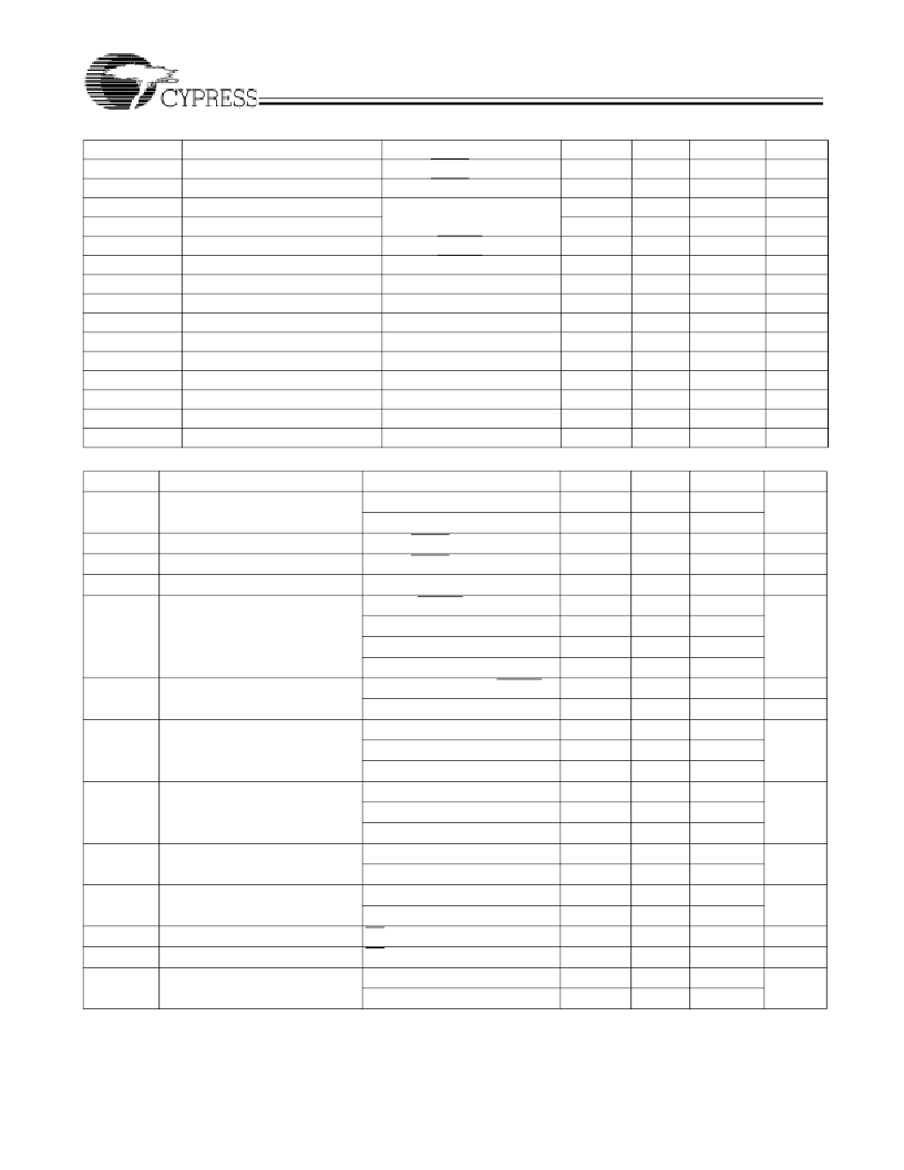
DC Electrical Specifications
(V
DD
= 2.5V ± 5%, T
A
= 0°C to +85°C)
Parameter
Description
V
PP
Input Peak-Peak Voltage
V
CMR
Input Common Mode Range
V
IL
Input Voltage, Low
V
IH
Input Voltage, High
V
OL
Output Voltage, Low
V
OH
Output Voltage, High
V
OL
V
OH
I
IL
I
IH
I
DDQ
Quiescent Supply Current
I
DD
Dynamic Supply Current
C
IN
Input Pin Capacitance
C
OUT
Output Pin Capacitance
Z
OUT
Output Impedance
AC Electrical Specifications
(V
DD
= 2.5V ± 5%, T
A
= 0°C to +85°C)
[5, 6]
Parameter
Description
f
in
Input Frequency
Condition
Min.
250
1.0
–0.30
1.7
0.2
V
DD
– 1.2
–0.3
1.8
–
–
–
–
–
–
–
Typ.
–
–
–
–
–
–
–
–
–
–
2.5
250
4
4
25
Max.
V
DD
– 1.3
V
DD
– 0.6
0.7
V
DD
+ 0.3
0.8
V
DD
– 0.4
0.6
V
DD
+ 0.3
–20
100
3.5
–
–
–
–
Unit
mV
V
V
V
V
V
V
V
μ
A
μ
A
mA
mA
pF
pF
PCLKI, PCLKI
PCLKI, PCLKI
OE, CLRDIV
PCLKO, PCLKO, 50
to V
TT
PCLKO, PCLKO, 50
to V
TT
I
OL
= 16 mA, QA, QB
I
OH
= –16 mA, QA, QB
V
IL
= V
SS
V
IH
= V
DD
V
IN
= 0V, outputs disabled
Outputs loaded @ 250 MHz
Output Voltage, Low
[3]
Output Voltage, High
[3]
Input Current, Low
[4]
Input Current, High
[4]
QA, QB
Condition
Min.
0
–
500
1.2
40
0
0
–
–
200
0.1
45
45
40
–
–
–
–
–
–
–
–
–
–
–
Typ.
–
–
–
–
–
–
–
–
–
–
–
–
–
–
50
150
200
–
–
–
–
3
3
|30|
–
Max.
320
250
1000
V
DD
– 0.6
60
320
160
80
250
700
1.2
55
55
60
75
200
250
7
7
7
7
6
6
|75|
|50|
Unit
MHz
CLRDIV = 0
CLRDIV = 1
PCLKI, PCLKI
PCLKI, PCLKI
V
PP
(AC)
V
CMR
(AC)
f
refDC
f
max
Input Peak-Peak Voltage
Input Common Mode Range
Reference Input Duty Cycle
Output Frequency
mV
V
%
MHz
PCLKO, PCLKO
Bank B, CLRDIV = 0
Bank A, CLRDIV = 0
Bank A, Bank B, CLRDIV = 1
20% to 80%, PCLKO, PCLKO
0.6V to 1.8V, QA, QB
t
r,
t
f
Output Rise/Fall Time
ps
ns
%
DC
Output Duty Cycle, DC
REF
= 50% Bank A/Bank B
LVPECL Output, fmax < 300 MHz
LVPECL Output, fmax > 300 MHz
Skew within Bank
BankA to BankB Skew
PECL Output to all Banks Skew
PCLKI to PCLKO
PCLKI to QA/QB
PCLKI to PCLKO
PCLKI to QA/QB
OE to any output
OE to any output
LVPECL output
LVTTL output
t
sk(O)
Output-to-Output Skew
ps
T
PLH
Propagation Delay
ns
T
PHL
Propagation Delay
ns
t
Qoff
t
Qon
t
JIT(CC)
Output Disable Time
Output Enable Time
Cycle-to-Cycle Jitter
ns
ns
ps
Notes:
3.
4.
5.
6.
Driving 50
parallel terminated transmission line to a termination voltage of V
TT
.
Inputs have pull-down resistors that affect the input current.
AC characteristics apply for parallel output termination to V
. Parameters are guaranteed by characterization and are not 100% tested.
AC test are measured with f
in
= 250 MHz at VDD/2 unless otherwise specified.
相關(guān)PDF資料 |
PDF描述 |
|---|---|
| CY2PP3115 | Clocks and Buffers |
| CY2PP318 | Clocks and Buffers |
| CY2PP3210 | Clocks and Buffers |
| CY2PP3220 | Clocks and Buffers |
| CY2PP326 | Clocks and Buffers |
相關(guān)代理商/技術(shù)參數(shù) |
參數(shù)描述 |
|---|---|
| CY2PD817ZC | 制造商:Rochester Electronics LLC 功能描述: 制造商:Cypress Semiconductor 功能描述: |
| CY2PD817ZCT | 制造商:CYPRESS 制造商全稱:Cypress Semiconductor 功能描述:320-MHz 1:7 PECL to PECL/CMOS Buffer |
| CY2PP3115 | 制造商:未知廠家 制造商全稱:未知廠家 功能描述:Clocks and Buffers |
| CY2PP3115AI | 制造商:CYPRESS 制造商全稱:Cypress Semiconductor 功能描述:1:15 Differential Fanout Buffer |
| CY2PP3115AIT | 制造商:CYPRESS 制造商全稱:Cypress Semiconductor 功能描述:1:15 Differential Fanout Buffer |
發(fā)布緊急采購,3分鐘左右您將得到回復(fù)。