- 您現(xiàn)在的位置:買(mǎi)賣(mài)IC網(wǎng) > PDF目錄378482 > CY28326OXCT (CYPRESS SEMICONDUCTOR CORP) Single Pole Normally Open: 1-Form-A PDF資料下載
參數(shù)資料
| 型號(hào): | CY28326OXCT |
| 廠商: | CYPRESS SEMICONDUCTOR CORP |
| 元件分類: | XO, clock |
| 英文描述: | Single Pole Normally Open: 1-Form-A |
| 中文描述: | 333.3 MHz, PROC SPECIFIC CLOCK GENERATOR, PDSO48 |
| 封裝: | LEAD FREE, SSOP-48 |
| 文件頁(yè)數(shù): | 2/23頁(yè) |
| 文件大?。?/td> | 288K |
| 代理商: | CY28326OXCT |
第1頁(yè)當(dāng)前第2頁(yè)第3頁(yè)第4頁(yè)第5頁(yè)第6頁(yè)第7頁(yè)第8頁(yè)第9頁(yè)第10頁(yè)第11頁(yè)第12頁(yè)第13頁(yè)第14頁(yè)第15頁(yè)第16頁(yè)第17頁(yè)第18頁(yè)第19頁(yè)第20頁(yè)第21頁(yè)第22頁(yè)第23頁(yè)
CY28326
Document #: 38-07616 Rev. *A
Page 2 of 23
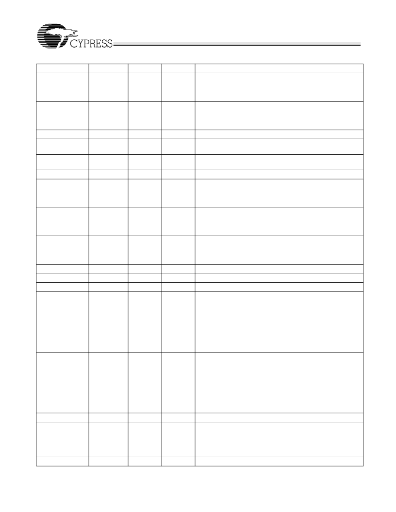
Pin Definition
Pin No.
1
Name
PWR
Type
I/O
Description
**FSA/REF0
VDDREF
Power-on Bi-directional Input/Output.
At power-up, FSA is the
input. when VTT_PWRGD transitions to a logic high, FSA state is
latched and this pin becomes REF0, buffered output copy of the
device’s XIN clock. Default Internal pull down.
Power-on Bi-directional Input/Output.
At power-up, FSB is the
input. when VTT_PWRGD transitions to a logic high, FSB state is
latched and this pin becomes REF1, buffered output copy of the
device’s XIN clock. Default Internal pull down.
3.3V Power supply for REF clock output.
Oscillator Buffer Input.
Connect to a crystal or to an external
clock.
Oscillator Buffer Input.
Connect to a crystal. Do not connect
when an external clock is applied at XIN.
Ground for REF clock outputs
Power-on Bi-directional Input/ Output.
At power up, FSC is the
input. When the VTT_PWRGD transitions to a logic high, FSC
state is latched and this pin becomes PCIF0. Default Internal pull
up.
Power-on Bi-directional Input/ Output.
At power up, FSD is the
input. When the VTT_PWRGD transitions to a logic high, FSD
state is latched and this pin becomes PCIF. Default Internal pull
up.
Power-on Bi-directional Input/ Output.
At power up,
MODE/PCIF2 is the input. When the power up, MODE state is
latched and then pin9 becomes PCIF2, PCI clock output for PCI
Device.Default pull-up, See
Table 2
3.3V power supply for PCI clock output.
Ground for PCI clock output.
PCI clock outputs.
Ratio0 Output/PCI5 Output.
At power up when RatioSel (pin 26)
strapping = “High” & MODE (pin 9) strapping=”High”, (PCI_STP#)
Ratio0/PCI5 becomes PCI5 clock output. At power up when
RatioSel (pin 26) strapping = “l(fā)ow” & MODE (pin 9) strapping
=”High”, (PCI_STP#)Ratio0/PCI5 becomes Ratio0 output to
support North bridge over freq strapping function. Once
MODE(pin 9) strapping=”Low”, then (PCI_STP#)Ratio0/PCI5
becomes PCI_STP#, Default = “PCI5” see
Table 2
, Default
Internal pull up.
Ratio1 Output/PCI6 Output.
At power up when RatioSel(pin 26)
strapping = “High” & MODE(pin 9) strapping=”High”, (CPU_STP#)
Ratio1/PCI6 becomes PCI6 clock output. At power up when
RatioSel (pin 26) strapping = “l(fā)ow” & MODE(pin 9) strapping
=”High”, (PCI_STP#)Ratio1/PCI6 becomes Ratio1 output to
support North bridge over freq strapping function. Once
MODE(pin 9) strapping=”Low”, then (PCI_STP#)Ratio1/PCI6
becomes CPU_STP#, Default = “PCI6” see
Table 2
, Default
Internal pull up.
48 MHz Clock Output.
Power-on Bi-directional Input/output.
At power up 24_48_SEL
is the input. When VTT_PWRGD is transited to logic high,
24_48_SEL state is latched and this pin becomes 24/48 MHz
output, Default 24_48_SEL= “0”, 48 MHz output.Default Internal
pull down.
Ground for 48 MHz clock output.
2
**FSB/REF1
VDDREF
I/O
3
4
VDDREF
XIN
I
I
VDDREF
5
XOUT
VDDREF
O
6
7
VSSREF
*FSC/PCIF0
PWR
I/O
VDDPCI
8
*FSD/PCIF1
VDDPCI
I/O
9
*MODE/
PCIF2
VDDPCI
I/O
10,17
11,18
VDDPCI
VSSPCI
PCI[0:4]
*(PCI_STP#)
Ratio0/PCI5
I
I
12,13,14,15,16
19
O
O
VDDPCI
20
*(CPU_STP#)
Ratio1/PCI6
VDDPCI
O
21
22
48 MHz
**24_48_SEL/
24_48 MHz
VDD48
VDD48
O
I/O
23
VSS48
I
相關(guān)PDF資料 |
PDF描述 |
|---|---|
| CY28341-2 | Universal Clock Chip for VIA P4M/KT/KM400 DDR Systems |
| CY29962 | 2.5V/3.3V, 150-MHz Multi-Output Zero Delay Buffer |
| CY30 | Sensor interface for an inductive engine wheel speed single rotation sensor |
| CY37128V | 5V, 3.3V, ISR⑩ High-Performance CPLDs |
| CY37256V | 5V, 3.3V, ISR⑩ High-Performance CPLDs |
相關(guān)代理商/技術(shù)參數(shù) |
參數(shù)描述 |
|---|---|
| CY28326SPC | 制造商:Cypress Semiconductor 功能描述: |
| CY28329 | 制造商:SPECTRALINEAR 制造商全稱:SPECTRALINEAR 功能描述:133 MHz Spread Spectrum Clock Synthesizer/Driver with Differential CPU Outputs |
| CY28329OXC | 功能描述:時(shí)鐘驅(qū)動(dòng)器及分配 Intel CK-408B for Plumas chipset RoHS:否 制造商:Micrel 乘法/除法因子:1:4 輸出類型:Differential 最大輸出頻率:4.2 GHz 電源電壓-最大: 電源電壓-最小:5 V 最大工作溫度:+ 85 C 封裝 / 箱體:SOIC-8 封裝:Reel |
| CY28329OXCT | 功能描述:時(shí)鐘驅(qū)動(dòng)器及分配 Intel CK-408B for Plumas chipset RoHS:否 制造商:Micrel 乘法/除法因子:1:4 輸出類型:Differential 最大輸出頻率:4.2 GHz 電源電壓-最大: 電源電壓-最小:5 V 最大工作溫度:+ 85 C 封裝 / 箱體:SOIC-8 封裝:Reel |
| CY28329PVC | 制造商:Cypress Semiconductor 功能描述: |
發(fā)布緊急采購(gòu),3分鐘左右您將得到回復(fù)。