- 您現(xiàn)在的位置:買賣IC網(wǎng) > PDF目錄223633 > CX72301-11 (SKYWORKS SOLUTIONS INC) PLL FREQUENCY SYNTHESIZER, 1000 MHz, PDSO28 PDF資料下載
參數(shù)資料
| 型號: | CX72301-11 |
| 廠商: | SKYWORKS SOLUTIONS INC |
| 元件分類: | PLL合成/DDS/VCOs |
| 英文描述: | PLL FREQUENCY SYNTHESIZER, 1000 MHz, PDSO28 |
| 封裝: | EXPOSED PAD, TSSOP-28 |
| 文件頁數(shù): | 7/20頁 |
| 文件大小: | 165K |
| 代理商: | CX72301-11 |
DATA SHEET CX72301
Skyworks Solutions, Inc. Phone [781] 376-3000 Fax [781] 376-3100 sales@skyworksinc.com www.skyworksinc.com
101090H Skyworks Proprietary and Confidential information Products and Product Information are Subject to Change Without Notice July 21, 2004
15
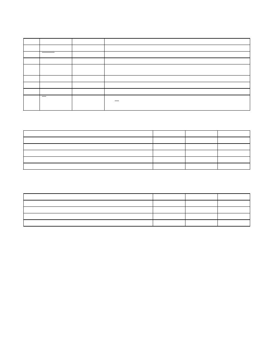
Table 5. CX72301 Signal Descriptions (2 of 2)
Pin #
Pin Name
Type
Description
21
GNDcp_aux (Note 1)
Power and ground
Auxiliary charge pump ground.
22
Fvco_aux
Input
Auxiliary VCO complimentary differential input.
23
Fvco_aux
Input
Auxiliary VCO differential input.
24
VCCcml_aux
(Note 1)
Power and ground
ECL/CML 3 V. Removing power safely powers down the associated divider chain and charge pump.
25
GNDdigital (Note 1)
Power and ground
Digital ground.
26
VCCdigital (Note 1)
Power and ground
Digital 3 V.
27
Data
Digital input
Serial address and data input pin. Address bits are followed by data bits.
28
CS
Digital input
Active low enable pin. Enables loading of address and data on the Data pin on the rising edge of Clock.
When CS goes high, data is transferred to the register indicated by the address. Subsequent clock edges
are ignored.
Note 1: Associated pairs of power and ground pins must be decoupled using 0.1
F capacitors.
Table 6. Absolute Maximum Ratings
Parameter
Min
Max
Units
Maximum analog RF supply voltage
3.6
VDC
Maximum digital supply voltage
3.6
VDC
Maximum charge pump supply voltage
5.25
VDC
Storage temperature
–65
+150
°C
Operating temperature
–40
+85
°C
Note:
Exposure to maximum rating conditions for extended periods may reduce device reliability. There is no damage to device with only one parameter set at the limit and all other
parameters set at or below their nominal values.
Table 7. Recommended Operating Conditions
Parameter
Min
Max
Units
Analog RF supplies
2.7
3.3
VDC
Digital supply
2.7
3.3
VDC
Charge pump supplies
2.7
5.0
VDC
Operating temperature (TA)
–40
+85
°C
相關(guān)PDF資料 |
PDF描述 |
|---|---|
| CX74017 | On the Direct Conversion Receiver |
| CX74038-12 | 2.6 GHz/800 MHz Dual Fractional-N/lnteger-N Frequency Synthesizer |
| CX77105-16P | Power Amplifier Module for CDMA/AMPS (824-849 MHz) |
| CX77107-14P | PA Module for CDMA / PCS (1850-1910 MHz) |
| CX77304-15 | 2MM SOCKET STRIPS |
相關(guān)代理商/技術(shù)參數(shù) |
參數(shù)描述 |
|---|---|
| CX72302 | 制造商:未知廠家 制造商全稱:未知廠家 功能描述:CX72302: Spur-Free, 6.1 GHz Dual Fractional-N Frequency Synthesizer |
| CX72303 | 制造商:未知廠家 制造商全稱:未知廠家 功能描述:CX72303 1.8 V Ultra Low Power Bluetooth? RF Tx|Bluetooth? RF Transceiver |
| CX725 2HDG | 制造商:Thomas & Betts 功能描述:EXTENDED PIPE CLAMP |
| CX7352-000 | 制造商:TE Connectivity 功能描述:RT-1145-OX-29-0-CS6450 - Bag |
| CX7354-000 | 制造商:TE Connectivity 功能描述:D-436-83CS2621 |
發(fā)布緊急采購,3分鐘左右您將得到回復(fù)。