- 您現(xiàn)在的位置:買賣IC網(wǎng) > PDF目錄4068 > CS80C286-16 (Intersil)IC CPU 16BIT 5V 16MHZ 68-PLCC PDF資料下載
參數(shù)資料
| 型號(hào): | CS80C286-16 |
| 廠商: | Intersil |
| 文件頁數(shù): | 34/60頁 |
| 文件大?。?/td> | 0K |
| 描述: | IC CPU 16BIT 5V 16MHZ 68-PLCC |
| 標(biāo)準(zhǔn)包裝: | 126 |
| 處理器類型: | 80C286 16-位 |
| 速度: | 16MHz |
| 電壓: | 5V |
| 安裝類型: | 表面貼裝 |
| 封裝/外殼: | 68-LCC(J 形引線) |
| 供應(yīng)商設(shè)備封裝: | 68-PLCC(24.23x24.23) |
| 包裝: | 管件 |
第1頁第2頁第3頁第4頁第5頁第6頁第7頁第8頁第9頁第10頁第11頁第12頁第13頁第14頁第15頁第16頁第17頁第18頁第19頁第20頁第21頁第22頁第23頁第24頁第25頁第26頁第27頁第28頁第29頁第30頁第31頁第32頁第33頁當(dāng)前第34頁第35頁第36頁第37頁第38頁第39頁第40頁第41頁第42頁第43頁第44頁第45頁第46頁第47頁第48頁第49頁第50頁第51頁第52頁第53頁第54頁第55頁第56頁第57頁第58頁第59頁第60頁

4
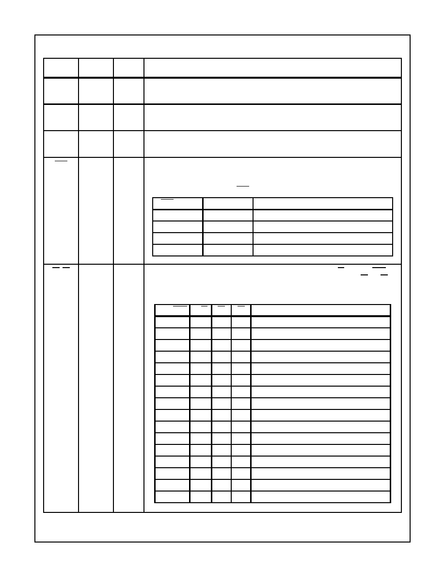
Pin Descriptions The following pin function descriptions are for the 80C286 microprocessor.
SYMBOL
PIN
NUMBER
TYPE
DESCRIPTION
CLK
31
I
SYSTEM CLOCK: provides the fundamental timing for the 80C286 system. It is divided by two inside
the 80C286 to generate the processor clock. The internal divide-by-two circuitry can be synchro-
nized to an external clock generator by a LOW to HIGH transition on the RESET input.
D15 - D0
36 - 51
I/O
DATA BUS: inputs data during memory, I/O, and interrupt acknowledge read cycles; outputs data
during memory and I/O write cycles. The data bus is active HIGH and is held at high impedance to
the last valid logic level during bus hold acknowledge.
A23 - A0
7 - 8
10 - 28
32 - 43
O
ADDRESS BUS: outputs physical memory and I/O port addresses. A23 - A16 are LOW during I/O
transfers. A0 is LOW when data is to be transferred on pins D7 - D0 (see table below). The address
bus is active High and floats to three-state off during bus hold acknowledge.
BHE
1
O
BUS HIGH ENABLE: indicates transfer of data on the upper byte of the data bus, D15 - D8. Eight-bit
oriented devices assigned to the upper byte of the data bus would normally use BHE to condition chip
select functions. BHE is active LOW and floats to three-state OFF during bus hold acknowledge.
S1, S0
4, 5
O
BUS CYCLE STATUS: indicates initiation of a bus cycle and along with M/IO and COD/lNTA, de-
fines the type of bus cycle. The bus is in a TS state whenever one or both are LOW. S1 and S0 are
active LOW and are held at a high impedance logic one during bus hold acknowledge.
BHE AND A0 ENCODINGS
BHE VALUE
A0 VALUE
FUNCTION
0
Word transfer
0
1
Byte transfer on upper half of data bus (D15 - D8)
1
0
Byte transfer on lower half of data bus (D7 - D0)
11
Reserved
80C286 BUS CYCLE STATUS DEFINITION
COD/INTA
M/IO
S1
S0
BUS CYCLE INITIATED
0(LOW)
0
Interrupt acknowledge
00
0
1
Reserved
00
1
0
Reserved
0
1
None; not a status cycle
0
1
0
If A1 = 1 then halt; else shutdown
0
1
0
1
Memory data read
0
1
0
Memory data write
0
1
None; not a status cycle
1(HIGH)
0
Reserved
1
0
1
I/O read
1
0
1
0
I/O write
1
0
1
None; not a status cycle
11
0
Reserved
1
0
1
Memory instruction read
11
1
0
Reserved
1
None; not a status cycle
80C286
相關(guān)PDF資料 |
PDF描述 |
|---|---|
| ACB90DHAR | CONN EDGECARD 180PS R/A .050 DIP |
| MPC857TZQ66B | IC MPU PWRQUICC 66MHZ 357-PBGA |
| ABB95DHAS | CONN EDGECARD 190PS R/A .050 SLD |
| MPC857TVR66B | IC MPU POWERQUICC 66MHZ 357-PBGA |
| MPC8271ZQTIEA | IC MPU POWERQUICC II 516-PBGA |
相關(guān)代理商/技術(shù)參數(shù) |
參數(shù)描述 |
|---|---|
| CS80C286-1696 | 制造商:Rochester Electronics LLC 功能描述:- Bulk |
| CS80C286-2 | 制造商:Harris Corporation 功能描述: |
| CS80C286-20 | 制造商:Rochester Electronics LLC 功能描述:- Bulk |
| CS80C286-2096 | 制造商:Rochester Electronics LLC 功能描述:- Bulk |
| CS80C286-20S2463 | 制造商:Rochester Electronics LLC 功能描述:- Bulk |
發(fā)布緊急采購,3分鐘左右您將得到回復(fù)。