- 您現(xiàn)在的位置:買賣IC網(wǎng) > PDF目錄170207 > CS5322GDWR28 (ON SEMICONDUCTOR) 1.5 A SWITCHING CONTROLLER, 1000 kHz SWITCHING FREQ-MAX, PDSO28 PDF資料下載
參數(shù)資料
| 型號: | CS5322GDWR28 |
| 廠商: | ON SEMICONDUCTOR |
| 元件分類: | 穩(wěn)壓器 |
| 英文描述: | 1.5 A SWITCHING CONTROLLER, 1000 kHz SWITCHING FREQ-MAX, PDSO28 |
| 封裝: | SOIC-28 |
| 文件頁數(shù): | 3/21頁 |
| 文件大小: | 405K |
| 代理商: | CS5322GDWR28 |
CS5322
http://onsemi.com
11
APPLICATIONS INFORMATION
FIXED FREQUENCY MULTIPHASE CONTROL
In a multiphase converter, multiple converters are
connected in parallel and are switched on at different times.
This reduces output current from the individual converters
and increases the apparent ripple frequency. Because several
converters are connected in parallel, output current can ramp
up or down faster than a single converter (with the same
value output inductor) and heat is spread among multiple
components.
The CS5322 uses a twophase, fixed frequency,
Enhanced V2 architecture. Each phase is delayed 180° from
the previous phase. Normally Gate(H) transitions high at the
beginning of each oscillator cycle. Inductor current ramps
up until the combination of the current sense signal and the
output ripple trip the PWM comparator and bring Gate(H)
low. Once Gate(H) goes low, it will remain low until the
beginning of the next oscillator cycle. While Gate(H) is
high, the enhanced V2 loop will respond to line and load
transients. Once Gate(H) is low, the loop will not respond
again until the beginning of the next cycle. Therefore,
constant frequency Enhanced V2 will typically respond
within the offtime of the converter.
The Enhanced V2 architecture measures and adjusts
current in each phase. An additional input (Cx) for inductor
current information has been added to the V2 loop for each
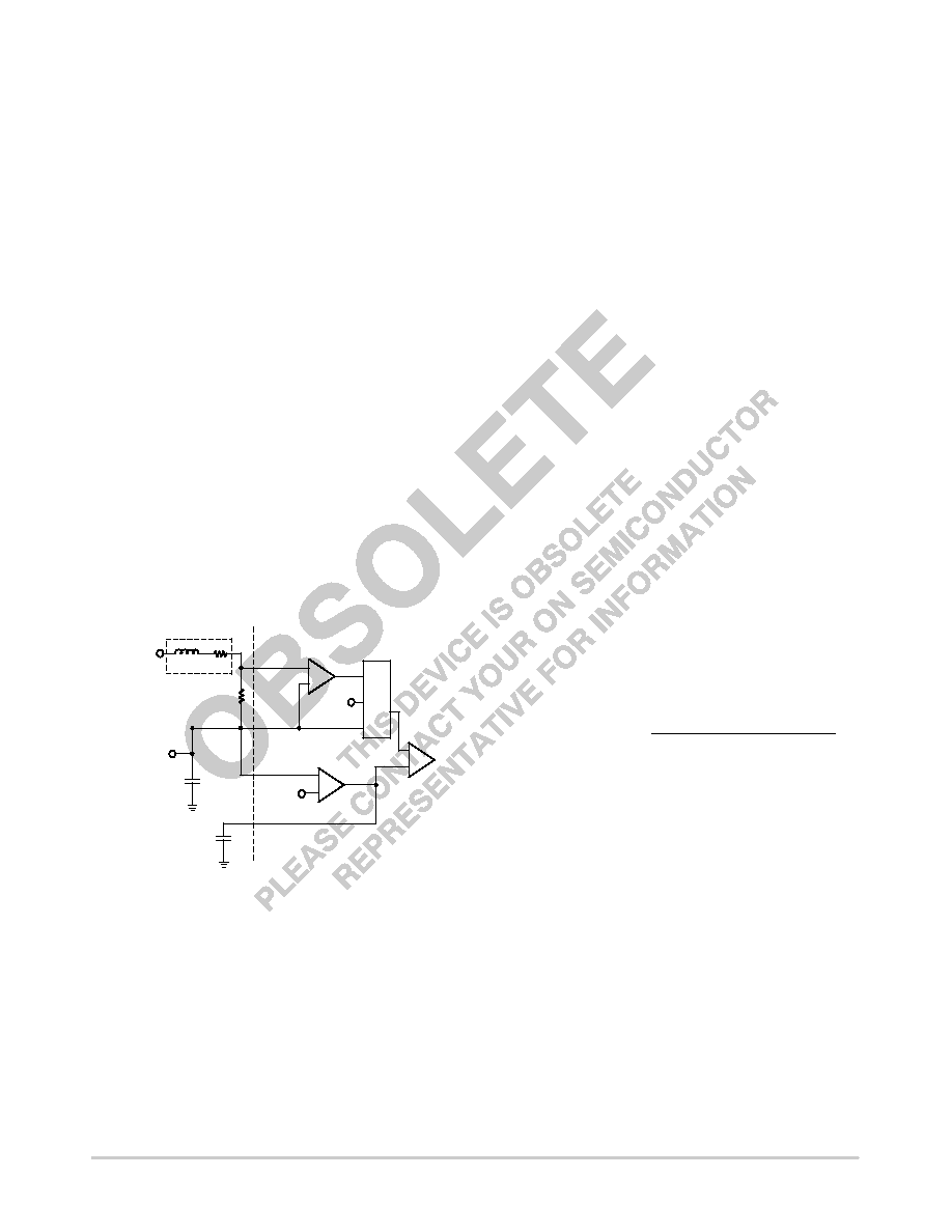
phase as shown in Figure 9.
Figure 9. Enhanced V2 Feedback and Current
Sense Scheme
CSREF
VOUT
SWNODE
CX
VFB
L
RL
RS
COMP
DACOUT
+
E.A.
+
OFFSET
CSA
PWM-
COMP
The inductor current is measured across RS, amplified by
CSA and summed with the OFFSET and Output Voltage at
the noninverting input of the PWM comparator. The
inductor current provides the PWM ramp and as inductor
current increases the voltage on the positive pin of the PWM
comparator rises and terminates the PWM cycle. If the
inductor starts the cycle with a higher current, the PWM
cycle will terminate earlier providing negative feedback.
The CS5322 provides a Cx input for each phase, but the
CSREF, VFB and COMP inputs are common to all phases.
Current sharing is accomplished by referencing all phases to
the same VFB and COMP pins, so that a phase with a larger
current signal will turn off earlier than phases with a smaller
current signal.
Including both current and voltage information in the
feedback signal allows the open loop output impedance of
the power stage to be controlled. When the average output
current is zero, the COMP pin will be only 1/2 of the steady
state ramp height plus the OFFSET above the output
voltage. If the COMP pin is held steady and the inductor
current changes, there must also be a change in the output
voltage. Or, in a closed loop configuration when the output
current changes, the COMP pin must move to keep the same
output voltage. The required change in the output voltage or
COMP pin depends on the scaling of the current feedback
signal and is calculated as
DV + RS
CSA Gain
DI
The singlephase power stage output impedance is:
Single Stage Impedance + DV DI + RS
CSA Gain.
The multiphase power stage output impedance is the
singlephase output impedance divided by the number of
phases. The output impedance of the power stage determines
how the converter will respond during the first few μs of a
transient before the feedback loop has repositioned the
COMP pin.
The peak output current of each phase can also be
calculated from;
Ipkout (per phase) +
VCOMP * VFB * VOFFSET
RS
CSA Gain
Figure 10 shows the step response of a single phase with
the COMP pin at a fixed level. Before T1 the converter is in
normal steady state operation. The inductor current provides
the PWM ramp through the Current Sense Amplifier. The
PWM cycle ends when the sum of the current signal, voltage
signal and OFFSET exceed the level of the COMP pin. At
T1 the output current increases and the output voltage sags.
The next PWM cycle begins and the cycle continues longer
than previously while the current signal increases enough to
make up for the lower voltage at the VFB pin and the cycle
ends at T2. After T2 the output voltage remains lower than
at light load and the current signal level is raised so that the
sum of the current and voltage signal is the same as with the
original load. In a closed loop system the COMP pin would
相關PDF資料 |
PDF描述 |
|---|---|
| CS5361GD16 | 2 A BATTERY CHARGE CONTROLLER, 635 kHz SWITCHING FREQ-MAX, PDSO16 |
| CS8413 | 96 KHZ DIGITAL AUDIO RECEIVER |
| CS8413-CS | 96 KHZ DIGITAL AUDIO RECEIVER |
| CS8414 | 96 KHZ DIGITAL AUDIO RECEIVER |
| CS8414-CS | 96 KHZ DIGITAL AUDIO RECEIVER |
相關代理商/技術參數(shù) |
參數(shù)描述 |
|---|---|
| CS5322-KL | 制造商:CIRRUS 制造商全稱:Cirrus Logic 功能描述:24-Bit Variable Bandwidth A/D Converter Chipset |
| CS5323 | 制造商:ONSEMI 制造商全稱:ON Semiconductor 功能描述:Three-Phase Buck Controller with 5-Bit DAC |
| CS5323/D | 制造商:未知廠家 制造商全稱:未知廠家 功能描述:Three-Phase Buck Controller with 5-Bit DAC |
| CS5323_06 | 制造商:ONSEMI 制造商全稱:ON Semiconductor 功能描述:Three−Phase Buck Controller with 5−Bit DAC |
| CS5323-BL | 制造商:未知廠家 制造商全稱:未知廠家 功能描述:Other/Special/Miscellaneous Converter |
發(fā)布緊急采購,3分鐘左右您將得到回復。