- 您現(xiàn)在的位置:買賣IC網(wǎng) > PDF目錄170207 > CS5322GDWR28 (ON SEMICONDUCTOR) 1.5 A SWITCHING CONTROLLER, 1000 kHz SWITCHING FREQ-MAX, PDSO28 PDF資料下載
參數(shù)資料
| 型號: | CS5322GDWR28 |
| 廠商: | ON SEMICONDUCTOR |
| 元件分類: | 穩(wěn)壓器 |
| 英文描述: | 1.5 A SWITCHING CONTROLLER, 1000 kHz SWITCHING FREQ-MAX, PDSO28 |
| 封裝: | SOIC-28 |
| 文件頁數(shù): | 19/21頁 |
| 文件大小: | 405K |
| 代理商: | CS5322GDWR28 |
CS5322
http://onsemi.com
7
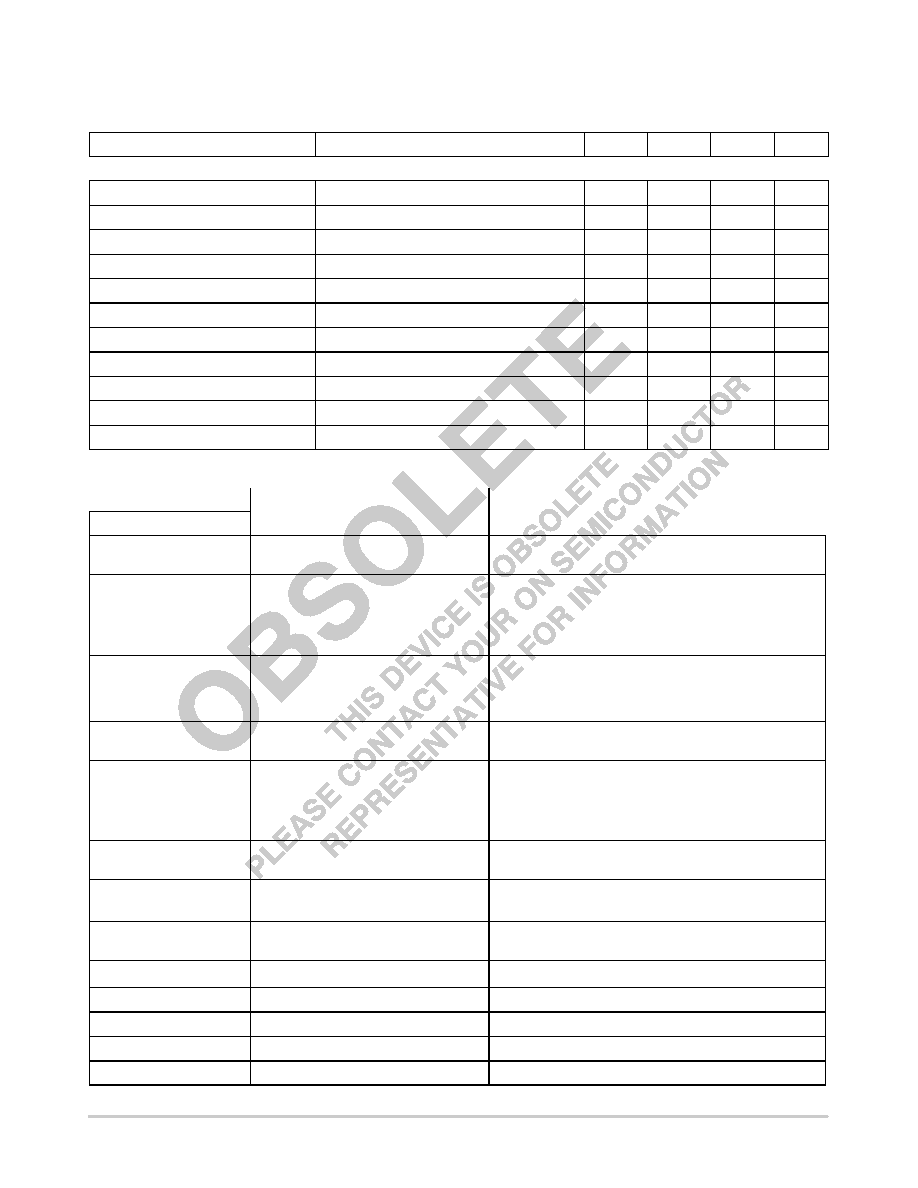
ELECTRICAL CHARACTERISTICS (continued) (0°C < TA < 70°C; 0°C < TJ < 125°C; 4.7 V < VCCL < 14 V; 8.0 V < VCCH < 20 V;
CGATE(H) = 3.3 nF, CGATE(L) = 3.3 nF, RR(OSC) = 32.4 k, CCOMP = 1.0 nF, CSS = 0.1 μF, CREF = 0.1 μF, DAC Code 10000, CVCC = 1.0 μF,
ILIM ≥ 1.0 V; unless otherwise specified.)
Characteristic
Unit
Max
Typ
Min
Test Conditions
General Electrical Specifications
VCCL Operating Current
VFB = COMP (no switching)
20
24.5
mA
VCCL1 Operating Current
VFB = COMP (no switching)
4.0
5.5
mA
VCCL2 Operating Current
VFB = COMP (no switching)
4.0
5.5
mA
VCCH1 Operating Current
VFB = COMP (no switching)
2.8
4.0
mA
VCCH2 Operating Current
VFB = COMP (no switching)
2.5
3.5
mA
VCCL Start Threshold
GATEs switching, Soft Start charging
4.05
4.4
4.7
V
VCCL Stop Threshold
GATEs stop switching, Soft Start discharging
3.75
4.2
4.6
V
VCCL Hysteresis
GATEs not switching, Soft Start not charging
100
200
300
mV
VCCH1 Start Threshold
GATEs switching, Soft Start charging
1.8
2.0
2.2
V
VCCH1 Stop Threshold
GATEs stop switching, Soft Start discharging
1.55
1.75
1.90
V
VCCH1 Hysteresis
GATEs not switching, Soft Start not charging
100
200
300
mV
PACKAGE PIN DESCRIPTION
PACKAGE PIN #
PIN SYMBOL
FUNCTION
SO28L
1
COMP
Output of the error amplifier and input for the PWM
comparators.
2
VFB
Voltage Feedback Pin. To use Adaptive Voltage Positioning
(AVP) select an offset voltage at light load and connect a
resistor between VFB and VOUT. The input current of the VFB
pin and the resistor value determine output voltage offset for
zero output current. Short VFB to VOUT for no AVP.
3
VDRP
Current sense output for AVP. The offset of this pin above the
DAC voltage is proportional to the output current. Connect a
resistor from this pin to VFB to set amount AVP or leave this
pin open for no AVP.
45
CS1CS2
Current sense inputs. Connect current sense network for the
corresponding phase to each input.
6
CSREF
Reference for Current Sense Amplifiers. To balance input
offset voltages between the inverting and noninverting inputs
of the Current Sense Amplifiers, connect a resistor between
CSREF and the output voltage. The value should be 1/3 of
the value of the resistors connected to the CSx pins.
7
PWRGD
Power Good Output. Open collector output goes low when
CSREF is out of regulation.
812
VID4VID0
Voltage ID DAC inputs. These pins are internally pulled up to
3.3 V if left open.
13
ILIM
Sets threshold for current limit. Connect to reference through
a resistive divider.
14
REF
Reference output. Decouple with 0.1 μF to LGND.
15
VCCH2
Power for GATE(H)2.
16
GATE(H)2
High side driver #2.
17
GND2
Return for #2 driver.
18
GATE(L)2
Low side driver #2.
相關PDF資料 |
PDF描述 |
|---|---|
| CS5361GD16 | 2 A BATTERY CHARGE CONTROLLER, 635 kHz SWITCHING FREQ-MAX, PDSO16 |
| CS8413 | 96 KHZ DIGITAL AUDIO RECEIVER |
| CS8413-CS | 96 KHZ DIGITAL AUDIO RECEIVER |
| CS8414 | 96 KHZ DIGITAL AUDIO RECEIVER |
| CS8414-CS | 96 KHZ DIGITAL AUDIO RECEIVER |
相關代理商/技術參數(shù) |
參數(shù)描述 |
|---|---|
| CS5322-KL | 制造商:CIRRUS 制造商全稱:Cirrus Logic 功能描述:24-Bit Variable Bandwidth A/D Converter Chipset |
| CS5323 | 制造商:ONSEMI 制造商全稱:ON Semiconductor 功能描述:Three-Phase Buck Controller with 5-Bit DAC |
| CS5323/D | 制造商:未知廠家 制造商全稱:未知廠家 功能描述:Three-Phase Buck Controller with 5-Bit DAC |
| CS5323_06 | 制造商:ONSEMI 制造商全稱:ON Semiconductor 功能描述:Three−Phase Buck Controller with 5−Bit DAC |
| CS5323-BL | 制造商:未知廠家 制造商全稱:未知廠家 功能描述:Other/Special/Miscellaneous Converter |
發(fā)布緊急采購,3分鐘左右您將得到回復。