- 您現(xiàn)在的位置:買賣IC網(wǎng) > PDF目錄369480 > BQ4845P Fast Recovery Glass Passivated Rectifier Diodes PDF資料下載
參數(shù)資料
| 型號: | BQ4845P |
| 英文描述: | Fast Recovery Glass Passivated Rectifier Diodes |
| 中文描述: | 實時時鐘 |
| 文件頁數(shù): | 6/20頁 |
| 文件大?。?/td> | 1155K |
| 代理商: | BQ4845P |

This activity unconditionally write-protects the external
SRAM as V
CC
falls below V
PFD
. If a memory access is in
progress to the external SRAM during power-fail detec-
tion, that memory cycle continues to completion before
the memory is write-protected. If the memory cycle is
not terminated within time t
WPT
, the chip enable output
is unconditionally driven high, write-protecting the con-
trolled SRAM.
As the supply continues to fall past V
PFD
, an internal
switching device forces V
OUT
to the external backup en-
ergy source.
CE
OUT
is held high by the V
OUT
energy
source.
During power-up, V
OUT
is switched back to the 5V sup-
ply as V
CC
rises above the backup cell input voltage
sourcing V
OUT
. CE
OUT
is held inactive for time t
CER
af-
ter the power supply has reached V
PFD
, independent of
theCE
IN
input, toallow for processor stabilization.
During power-valid operation, the CE
IN
input is passed
through to the CE
OUT
output with a propagation delay of
less than 12ns.
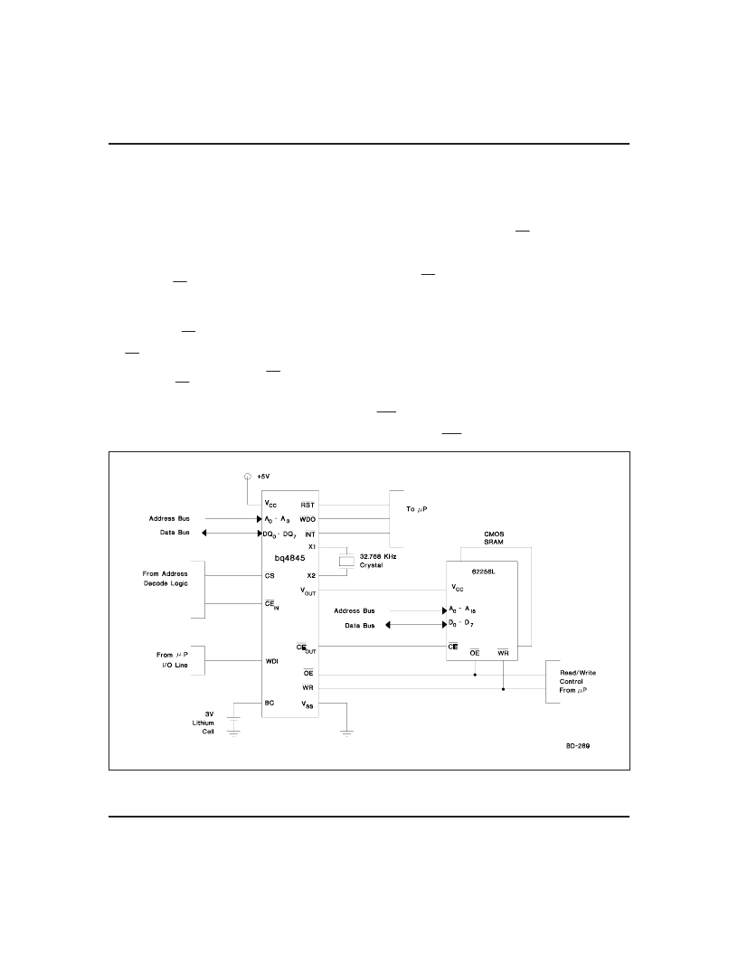
Figure 2 shows the hardware hookup for the external
RAM, battery, and crystal.
A
primary backup energy source input is provided on
the bq4845. The BC input accepts a 3V primary battery,
typically some type of lithium chemistry. Since the
bq4845 provides for reverse battery charging protection,
no diode or current limiting resistor is needed in series
with the cell. To prevent battery drain when there is no
valid data to retain, V
OUT
and CE
OUT
are internally iso-
lated from BC by the initial connection of a battery. Fol-
lowing the first application of V
CC
above V
PFD
, this iso-
lation is broken, and the backup cell provides power to
V
OUT
and CE
OUT
for theexternal SRAM.
The crystal should be located as close to X1 and X2 as
possible and meet the specifications in the Crystal
Specification Table. With the specified crystal, the
bq4845 RTC will be accurate to within one minute per
month at room temperature. In the absence of a crystal,
a 32.768 kHz waveform can be fed
grounded.
into X1 with X2
Power-On Reset
The bq4845 provides a power-on reset, which pulls the
RST pin low on power-down and remains low on power-
up for t
RST
after V
CC
passes V
PFD.
With valid battery
voltageon BC, RST remains valid for V
CC
= V
SS
.
6
Figure 2. bq4845 Application Circuit
Aug. 1995
bq4845/bq4845Y
Powered by ICminer.com Electronic-Library Service CopyRight 2003
相關(guān)PDF資料 |
PDF描述 |
|---|---|
| BQ4845S | Fast Recovery Glass Passivated Rectifier Diodes |
| BQ4845YP | Fast Recovery Glass Passivated Rectifier Diodes |
| BQ4845YS | Fast Recovery Glass Passivated Rectifier Diodes |
| BQ4847Y | Fast Recovery Glass Passivated Rectifier Diodes |
| BQ48S1.5-30A | Fast Recovery Glass Passivated Rectifier Diodes |
相關(guān)代理商/技術(shù)參數(shù) |
參數(shù)描述 |
|---|---|
| BQ4845P- | 制造商:TI 制造商全稱:Texas Instruments 功能描述:Parallel RTC With CPU Supervisor |
| BQ4845P-A4 | 功能描述:實時時鐘 w/NVSRAM Control Watchdog Timer RoHS:否 制造商:Microchip Technology 功能:Clock, Calendar. Alarm RTC 總線接口:I2C 日期格式:DW:DM:M:Y 時間格式:HH:MM:SS RTC 存儲容量:64 B 電源電壓-最大:5.5 V 電源電壓-最小:1.8 V 最大工作溫度:+ 85 C 最小工作溫度: 安裝風格:Through Hole 封裝 / 箱體:PDIP-8 封裝:Tube |
| BQ4845P-N | 制造商:TI 制造商全稱:Texas Instruments 功能描述:Parallel RTC With CPU Supervisor |
| BQ4845S | 制造商:未知廠家 制造商全稱:未知廠家 功能描述:Real-Time Clock |
| BQ4845S- | 制造商:TI 制造商全稱:Texas Instruments 功能描述:Parallel RTC With CPU Supervisor |
發(fā)布緊急采購,3分鐘左右您將得到回復(fù)。