- 您現(xiàn)在的位置:買賣IC網(wǎng) > PDF目錄42904 > ATF-55143-TR2G (AGILENT TECHNOLOGIES INC) C BAND, Si, N-CHANNEL, RF SMALL SIGNAL, HEMFET PDF資料下載
參數(shù)資料
| 型號(hào): | ATF-55143-TR2G |
| 廠商: | AGILENT TECHNOLOGIES INC |
| 元件分類: | 小信號(hào)晶體管 |
| 英文描述: | C BAND, Si, N-CHANNEL, RF SMALL SIGNAL, HEMFET |
| 封裝: | LEAD FREE, PLASTIC, SC-70, 4 PIN |
| 文件頁(yè)數(shù): | 17/21頁(yè) |
| 文件大小: | 235K |
| 代理商: | ATF-55143-TR2G |
第1頁(yè)第2頁(yè)第3頁(yè)第4頁(yè)第5頁(yè)第6頁(yè)第7頁(yè)第8頁(yè)第9頁(yè)第10頁(yè)第11頁(yè)第12頁(yè)第13頁(yè)第14頁(yè)第15頁(yè)第16頁(yè)當(dāng)前第17頁(yè)第18頁(yè)第19頁(yè)第20頁(yè)第21頁(yè)
5
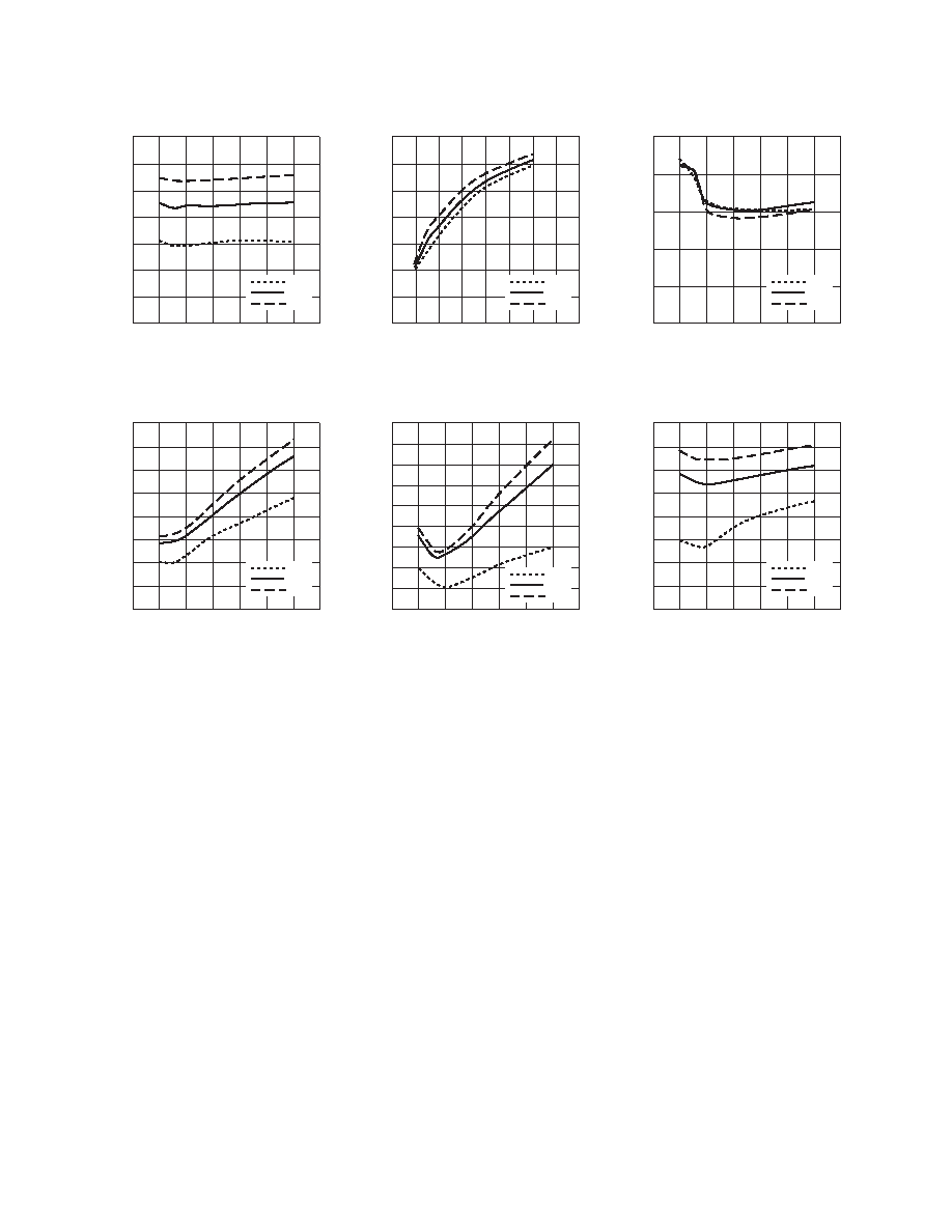
ATF-55143 Typical Performance Curves, continued
Figure 15. P1dB vs. Idq and Vds at 2 GHz.
[1,2]
Idq (mA)
P1dB
(dBm)
035
2V
2.7V
3V
10
520
25
30
15
17
16
15
14
13
12
11
10
Figure 16. Gain vs. Ids and Vds at 900 MHz.
[1]
Ids (mA)
GAIN
(dB)
040
20
10
515
25
35
30
2V
2.7V
3V
25
24
23
22
21
20
19
18
Figure 18. OIP3 vs. Ids and Vds at 900 MHz.
[1]
Ids (mA)
OIP3
(dBm)
035
32
30
28
26
24
22
20
18
16
2V
2.7V
3V
10
520
25
30
15
Figure 19. IIP3 vs. Ids and Vds at 900 MHz.
[1]
Ids (mA)
IIP3
(dBm)
035
7
6
5
4
3
2
1
0
-1
-2
2V
2.7V
3V
10
520
25
30
15
Figure 20. P1dB vs. Idq and Vds at
900 MHz.[1,2]
Idq (mA)
P1dB
(dBm)
035
17
16
15
14
13
12
11
10
9
2V
2.7V
3V
10
520
25
30
15
Figure 17. Fmin vs. Ids and Vds at 900 MHz.
Ids (mA)
Fmin
(dB)
035
2V
2.7V
3V
10
520
25
30
15
0.35
0.30
0.25
0.20
0.15
0.10
Notes:
1. Measurements at 2 GHz were made on a
fixed tuned production test board that was
tuned for optimal OIP3 match with reasonable
noise figure at 2.7 V, 10 mA bias. This circuit
represents a trade-off between optimal noise
match, maximum OIP3 match and a realizable
match based on production test board
requirements. Measurements taken above
and below 2 GHz were made using a double
stub tuner at the input tuned for low noise
and a double stub tuner at the output tuned
for maximum OIP3. Circuit losses have been
de-embedded from actual measurements.
2. P1dB measurements are performed with
passive biasing. Quiescent drain current, I
dsq,
is set with zero RF drive applied. As P1dB is
approached, the drain current may increase or
decrease depending on frequency and dc bias
point. At lower values of Idsq, the device is
running close to class B as power output
approaches P1dB. This results in higher P1dB
and higher PAE (power added efficiency)
when compared to a device that is driven by a
constant current source as is typically done
with active biasing. As an example, at a V
DS =
2.7V and I
dsq = 5 mA, Id increases to 15 mA as
a P1dB of +14.5 dBm is approached.
相關(guān)PDF資料 |
PDF描述 |
|---|---|
| ATF-55143-BLK | C BAND, Si, N-CHANNEL, RF SMALL SIGNAL, HEMFET |
| ATF-55143-TR2G | C BAND, Si, N-CHANNEL, RF SMALL SIGNAL, HEMFET |
| ATF-55143-BLKG | C BAND, Si, N-CHANNEL, RF SMALL SIGNAL, HEMFET |
| ATF-55143-TR1G | C BAND, Si, N-CHANNEL, RF SMALL SIGNAL, HEMFET |
| ATF-55143-TR2 | C BAND, Si, N-CHANNEL, RF SMALL SIGNAL, HEMFET |
相關(guān)代理商/技術(shù)參數(shù) |
參數(shù)描述 |
|---|---|
| ATF-551M4 | 制造商:AGILENT 制造商全稱:AGILENT 功能描述:Low Noise Enhancement Mode Pseudomorphic HEMT in a Miniature Leadless Package |
| ATF-551M4-BLK | 功能描述:射頻GaAs晶體管 Transistor GaAs Single Voltage RoHS:否 制造商:TriQuint Semiconductor 技術(shù)類型:pHEMT 頻率:500 MHz to 3 GHz 增益:10 dB 噪聲系數(shù): 正向跨導(dǎo) gFS(最大值/最小值):4 S 漏源電壓 VDS: 閘/源擊穿電壓:- 8 V 漏極連續(xù)電流:3 A 最大工作溫度:+ 150 C 功率耗散:10 W 安裝風(fēng)格: 封裝 / 箱體: |
| ATF-551M4-BLK | 制造商:Avago Technologies 功能描述:Transistor |
| ATF-551M4-TR1 | 功能描述:射頻GaAs晶體管 Transistor GaAs Single Voltage RoHS:否 制造商:TriQuint Semiconductor 技術(shù)類型:pHEMT 頻率:500 MHz to 3 GHz 增益:10 dB 噪聲系數(shù): 正向跨導(dǎo) gFS(最大值/最小值):4 S 漏源電壓 VDS: 閘/源擊穿電壓:- 8 V 漏極連續(xù)電流:3 A 最大工作溫度:+ 150 C 功率耗散:10 W 安裝風(fēng)格: 封裝 / 箱體: |
| ATF-551M4-TR2 | 功能描述:射頻GaAs晶體管 Transistor GaAs Single Voltage RoHS:否 制造商:TriQuint Semiconductor 技術(shù)類型:pHEMT 頻率:500 MHz to 3 GHz 增益:10 dB 噪聲系數(shù): 正向跨導(dǎo) gFS(最大值/最小值):4 S 漏源電壓 VDS: 閘/源擊穿電壓:- 8 V 漏極連續(xù)電流:3 A 最大工作溫度:+ 150 C 功率耗散:10 W 安裝風(fēng)格: 封裝 / 箱體: |
發(fā)布緊急采購(gòu),3分鐘左右您將得到回復(fù)。