- 您現(xiàn)在的位置:買賣IC網(wǎng) > PDF目錄42904 > ATF-55143-TR1 C BAND, Si, N-CHANNEL, RF SMALL SIGNAL, HEMFET PDF資料下載
參數(shù)資料
| 型號: | ATF-55143-TR1 |
| 元件分類: | 小信號晶體管 |
| 英文描述: | C BAND, Si, N-CHANNEL, RF SMALL SIGNAL, HEMFET |
| 封裝: | PLASTIC, SC-70, 4 PIN |
| 文件頁數(shù): | 6/21頁 |
| 文件大小: | 254K |
| 代理商: | ATF-55143-TR1 |
14
ATF-55143 Applications Information
Introduction
Avago Technologies’ ATF55143 is a low noise
enhancement mode PHEMT designed for use in low cost
commercial applications in the VHF through 6 GHz fre
quency range. As opposed to a typical depletion mode
PHEMT where the gate must be made negative with
respect to the source for proper operation, an enhance
ment mode PHEMT requires that the gate be made more
positive than the source for normal operation. Therefore
a negative power supply voltage is not required for an
enhancement mode device. Biasing an enhancement
mode PHEMT is much like biasing the typical bipolar
junction transistor. Instead of a 0.7V base to emitter volt
age, the ATF55143 enhancement mode PHEMT requires
about a 0.47V potential between the gate and source for
a nominal drain current of 10 mA.
Matching Networks
The techniques for impedance matching an enhance
ment mode device are very similar to those for matching
a depletion mode device. The only difference is in the
method of supplying gate bias. S and Noise Parameters
for various bias conditions are listed in this data sheet.
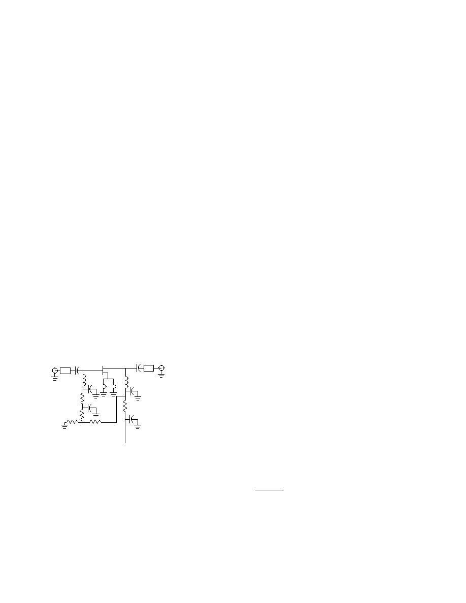
The circuit shown in Figure 1 shows a typical LNA cir
cuit normally used for 900 and 1900 MHz applications
(Consult the Avago Technologies website for application
notes covering specific applications). High pass imped
ance matching networks consisting of L1/C1 and L4/C4
provide the appropriate match for noise figure, gain, S11
and S22. The high pass structure also provides low fre
quency gain reduction which can be beneficial from the
standpoint of improving outofband rejection.
INPUT
C1
C2
C3
L1
R4
R1
R2
Vdd
R3
L2
L3
L4
Q1
Zo
C4
C5
C6
OUTPUT
R5
Figure1.TypicalATF-55143LNAwithPassiveBiasing.
Capacitors C2 and C5 provide a low impedance inband
RF bypass for the matching networks. Resistors R3 and
R4 provide a very important low frequency termination
for the device. The resistive termination improves low
frequency stability. Capacitors C3 and C6 provide the
low frequency RF bypass for resistors R3 and R4. Their
value should be chosen carefully as C3 and C6 also pro
vide a termination for low frequency mixing products.
These mixing products are as a result of two or more in
band signals mixing and producing third order inband
distortion products. The low frequency or difference
mixing products are terminated by C3 and C6. For best
suppression of third order distortion products based on
the CDMA 1.25 MHz signal spacing, C3 and C6 should
be 0.1 F in value. Smaller values of capacitance will
not suppress the generation of the 1.25 MHz difference
signal and as a result will show up as poorer two tone
IP3 results.
Bias Networks
One of the major advantages of the enhancement
mode technology is that it allows the designer to be
able to dc ground the source leads and then merely
apply a positive voltage on the gate to set the desired
amount of quiescent drain current I
d.
Whereas a depletion mode PHEMT pulls maximum
drain current when V
gs = 0V, an enhancement mode
PHEMT pulls only a small amount of leakage current
when V
gs= 0 V. Only when Vgs is increased above Vth, the
device threshold voltage, will drain current start to flow.
At a V
ds of 2.7V and a nominal Vgs of 0.47 V, the drain
current I
d will be approximately 10 mA. The data sheet
suggests a minimum and maximum V
gs over which the
desired amount of drain current will be achieved. It is
also important to note that if the gate terminal is left
open circuited, the device will pull some amount of
drain current due to leakage current creating a voltage
differential between the gate and source terminals.
Passive Biasing
Passive biasing of the ATF55143 is accomplished by
the use of a voltage divider consisting of R1 and R2. The
voltage for the divider is derived from the drain voltage
which provides a form of voltage feedback through the
use of R3 to help keep drain current constant. Resis
tor R5 (approximately 10k) is added to limit the gate
current of enhancement mode devices such as the
ATF55143. This is especially important when the device
is driven to P
1dB or PSAT.
Resistor R3 is calculated based on desired V
ds, Ids and
available power supply voltage.
R3 =
V
DD – Vds
(1)
p
I
ds + IBB
V
DD is the power supply voltage.
V
ds is the device drain to source voltage.
I
ds is the desired drain current.
I
BB is the current flowing through the R1/R2 resistor volt
age divider network.
相關(guān)PDF資料 |
PDF描述 |
|---|---|
| ATF-551M4-TR2G | X BAND, Si, N-CHANNEL, RF SMALL SIGNAL, HEMFET |
| ATF-551M4-BLK | X BAND, Si, N-CHANNEL, RF SMALL SIGNAL, HEMFET |
| ATF-551M4-BLKG | X BAND, Si, N-CHANNEL, RF SMALL SIGNAL, HEMFET |
| ATF-551M4-TR1 | X BAND, Si, N-CHANNEL, RF SMALL SIGNAL, HEMFET |
| ATF-551M4-TR2 | X BAND, Si, N-CHANNEL, RF SMALL SIGNAL, HEMFET |
相關(guān)代理商/技術(shù)參數(shù) |
參數(shù)描述 |
|---|---|
| ATF-55143-TR1G | 功能描述:射頻GaAs晶體管 Transistor GaAs Single Voltage RoHS:否 制造商:TriQuint Semiconductor 技術(shù)類型:pHEMT 頻率:500 MHz to 3 GHz 增益:10 dB 噪聲系數(shù): 正向跨導(dǎo) gFS(最大值/最小值):4 S 漏源電壓 VDS: 閘/源擊穿電壓:- 8 V 漏極連續(xù)電流:3 A 最大工作溫度:+ 150 C 功率耗散:10 W 安裝風(fēng)格: 封裝 / 箱體: |
| ATF-55143-TR2 | 制造商:AGILENT 制造商全稱:AGILENT 功能描述:Agilent ATF-55143 Low Noise Enhancement Mode Pseudomorphic HEMT in a Surface Mount Plastic Package |
| ATF-55143-TR2G | 功能描述:射頻GaAs晶體管 Transistor GaAs Single Voltage RoHS:否 制造商:TriQuint Semiconductor 技術(shù)類型:pHEMT 頻率:500 MHz to 3 GHz 增益:10 dB 噪聲系數(shù): 正向跨導(dǎo) gFS(最大值/最小值):4 S 漏源電壓 VDS: 閘/源擊穿電壓:- 8 V 漏極連續(xù)電流:3 A 最大工作溫度:+ 150 C 功率耗散:10 W 安裝風(fēng)格: 封裝 / 箱體: |
| ATF-551M4 | 制造商:AGILENT 制造商全稱:AGILENT 功能描述:Low Noise Enhancement Mode Pseudomorphic HEMT in a Miniature Leadless Package |
| ATF-551M4-BLK | 功能描述:射頻GaAs晶體管 Transistor GaAs Single Voltage RoHS:否 制造商:TriQuint Semiconductor 技術(shù)類型:pHEMT 頻率:500 MHz to 3 GHz 增益:10 dB 噪聲系數(shù): 正向跨導(dǎo) gFS(最大值/最小值):4 S 漏源電壓 VDS: 閘/源擊穿電壓:- 8 V 漏極連續(xù)電流:3 A 最大工作溫度:+ 150 C 功率耗散:10 W 安裝風(fēng)格: 封裝 / 箱體: |
發(fā)布緊急采購,3分鐘左右您將得到回復(fù)。