- 您現(xiàn)在的位置:買賣IC網(wǎng) > PDF目錄358668 > AT78C1505 (Atmel Corp.) DVD/CD Read Preamplifier(DVD/CD可讀前置放大器) PDF資料下載
參數(shù)資料
| 型號: | AT78C1505 |
| 廠商: | Atmel Corp. |
| 英文描述: | DVD/CD Read Preamplifier(DVD/CD可讀前置放大器) |
| 中文描述: | DVD / CD光碟讀取放大器(DVD / CD光碟可讀前置放大器) |
| 文件頁數(shù): | 3/12頁 |
| 文件大?。?/td> | 65K |
| 代理商: | AT78C1505 |
AT78C1505
3
Functional Description
ABCD High-Speed Transimpedance Amplifiers
The AT78C1505 contains four transimpedance amplifiers
for high-speed amplification of DVD/CD readback signals.
An application diagram for each input is shown below.
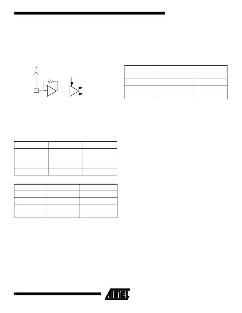
Photodetector and Fast Transimpedance Amplifier
Each transimpedance (TZ) stage is implemented as a
shunt feedback amplifier with a selectable feedback
resistor and additional programmable gain for flexible
single ended input current to differential output voltage
conversion. The following tables show TZ gains and PGC
selection.
Table 1.
High-Speed TZ Gain Selection
In addition to the coarse gain adjustment given above, a
fine transimpedance gain trim exists. This is a
±
15% trim
which applies to the overall gain independent of TZ and
PGC settings. This can be set using GAINTRM<1:0> via
REG 0 and is set according to the following table.
Table 3.
Overall Trim Setting
Offset DACs are provided to compensate for the DC
component of the photodiode currents. Each input channel
A, B, C and D has an offset DAC. The offset is introduced
after the transimpedance amplifier but before the
programable gain amplifier. This implies the offset
correction is scaled with PGC setting but not
transimpedance setting. Each channel offset correction
affects the channels respective output in addition to the RF
and TPP outputs. The RF/TPP outputs have 1/2 the gain of
the A, B, C and D outputs, thus the offsets appear as 1/2
the value at the RF/TPP outputs when compared to the A,
B, C and D outputs. Offsets on channel A input are nulled
by observing channel A output and choosing the
appropriate DAC value such that zero volts differential
results (AP - AN = 0). This also applies to channels B, C
and D. Six bits are provided for offset adjustment with one
LSB equal to -1.26mV on RF/TPP channels and -2.52mV
on A, B, C, and D channels (due to the factor of two
difference in the gains of these outputs). With 6 bits this
translates into a maximum of -80.6mV and -161.2mV
correction on RF/TPP and A/B/C/D outputs respectively.
Offset correction is negative in order to compensate for
positive input current offsets and the PGC amplifier is set to
a gain of 1V/V for the above correction values.
TZ<1>
TZ<0>
TZ Gain
0
0
3.1K
0
1
4.15K
1
0
12.7K
1
1
0.45K
Table 2.
High-Speed PGC Gain Selection
PGC<1>
PGC<0>
PGC V/V
0
0
0.5
0
1
0.7
1
0
1.0
1
1
2.0
PGC
A
TransZ Amp
R
TZ
-A
A
I
3 to 15V
offset
GAINTRM<1>
GAINTRM<0>
Overall Trim V/V
0
0
85%
0
1
100%
1
0
100%
1
1
115%
相關(guān)PDF資料 |
PDF描述 |
|---|---|
| ATF1500 | 44-pin Complex PLD(44腳復(fù)雜可編程邏輯器件) |
| ATF1516ASL | High-performance EE-based CPLD(高性能可電擦除復(fù)雜可編程邏輯器件(CPLD)) |
| ATtiny12L | 8-Bit AVR Microcontroller with 1K bytes Flash(8位AVR技術(shù)微控制器(帶1K字節(jié)閃速存儲器 )) |
| AXH010A0MZ | 1-OUTPUT 15 W DC-DC REG PWR SUPPLY MODULE |
| BA545AL | Low-leakage diode |
相關(guān)代理商/技術(shù)參數(shù) |
參數(shù)描述 |
|---|---|
| AT78C1507 | 制造商:ATMEL 制造商全稱:ATMEL Corporation 功能描述:DVD/CD Read Channel |
| AT78C4050 | 制造商:ATMEL 制造商全稱:ATMEL Corporation 功能描述:DVD PRML Channel and System Controller SoC |
| AT78C5009 | 制造商:ATMEL 制造商全稱:ATMEL Corporation 功能描述:Serial ATA Host Bridge |
| AT78C5010 | 制造商:ATMEL 制造商全稱:ATMEL Corporation 功能描述:SERIAL ATA HOST/DEVICE BRIDGE |
| AT78C5081 | 制造商:ATMEL 制造商全稱:ATMEL Corporation 功能描述:Serial ATA Physical Layer |
發(fā)布緊急采購,3分鐘左右您將得到回復(fù)。