- 您現(xiàn)在的位置:買賣IC網(wǎng) > PDF目錄362443 > AS4SD1M16S-8A x16 SDRAM PDF資料下載
參數(shù)資料
| 型號: | AS4SD1M16S-8A |
| 英文描述: | x16 SDRAM |
| 中文描述: | x16內(nèi)存 |
| 文件頁數(shù): | 27/51頁 |
| 文件大小: | 1071K |
| 代理商: | AS4SD1M16S-8A |
第1頁第2頁第3頁第4頁第5頁第6頁第7頁第8頁第9頁第10頁第11頁第12頁第13頁第14頁第15頁第16頁第17頁第18頁第19頁第20頁第21頁第22頁第23頁第24頁第25頁第26頁當(dāng)前第27頁第28頁第29頁第30頁第31頁第32頁第33頁第34頁第35頁第36頁第37頁第38頁第39頁第40頁第41頁第42頁第43頁第44頁第45頁第46頁第47頁第48頁第49頁第50頁第51頁
S DR A M
AS4SD16M16
Austin Semiconductor, Inc.
AS4SD16M16
Rev. 1.5 6/03
Austin Semiconductor, Inc. reserves the right to change products or specifications without notice.
27
*Stresses greater than those listed under "Absolute Maximum
Ratings" may cause permanent damage to the device. This is
a stress rating only and functional operation of the device at
these or any other conditions above those indicated in the
operation section of this specification is not implied. Exposure
to absolute maximum rating conditions for extended periods
may affect reliability.
**Junction temperature depends upon package type, cycle time,
loading, ambient temperature and airflow, and humidity (plas-
tics).
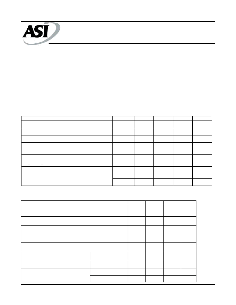
ABSOLUTE MAXIMUM RATINGS*
Voltage on V
DD
, V
DD
Q Supply
Relative to V
SS
...................................................-1V to +4.6V
Voltage on Inputs, NC or I/O Pins
Relative to V
SS
...................................................-1V to +4.6V
Operating Temperature, T
A
(IT)..................................-40°C to +85°C
Operating Temperature, T
A
(IT+)..............................-45°C to +105°C
Operating Temperature, T
(XT)..............................-55°C to +125°C
Storage Temperature (plastic)..................................-55°C to +150°C
Power Dissipation...........................................................................1W
ELECTRICAL CHARACTERISTICS AND RECOMMENDED DC OPERATING CONDITIONS
1,5,6
(V
DD
, V
DD
Q = +3.3V ±0.3V)
PARAMETER
SYMBOL
Supply Voltage
V
DD
, V
DD
Q
MIN
3
MAX
3.6
UNITS
V
NOTES
Input High Voltage: Logic 1; All inputs
V
IH
2.2
V
DD
+ 0.3
V
22
Input Low Voltage: Logic 0; All inputs
V
IL
-0.3
0.8
V
22
Input Leakage Current: Any input 0V < V
IN
< V
DD
(All other pins not under test = 0V)
Output Leakage Current: DQs are disabled:
0V < V
OUT
< V
DD
Q
Output Levels:
Output High Voltage (I
OUT
= -4mA)
I
I
-5
5
μA
I
OZ
-5
5
μA
V
OH
2.4
---
V
Output Low Voltage (I
OUT
= 4mA)
V
OL
---
0.4
V
I
DD
SPECIFICATIONS AND CONDITIONS
1,5,6,11,13
(V
DD
, V
DD
Q = +3.3V ±0.3V)
PARAMETER
Operating Current: Active Mode;
Burst = 2; READ or WRITE; t
RC
= t
RC
(MIN)
Standby Current: Power-Down Mode;
All banks idle; CKE = LOW
Standby Current: Active Mode;
CKE = HIGH; CS\ = HIGH; All banks active after t
RCD
met;
No accesses in progress
SYMBOL MAX (-75)
UNITS
NOTES
3, 18,
19, 32
I
DD1
140
mA
I
DD2
3
mA
32
I
DD3
45
mA
3, 12,
19, 32
I
DD4
150
mA
3, 18,
19, 32
t
RFC
= t
RFC
(MIN)
I
DD5
300
mA
t
RFC
= 7.81 μs
I
DD6
6
mA
Standard
I
DD7
4
mA
4, 35
Low Power (L)
I
DD7
3
mA
35
Operating Current: Burst Mode; Continuous Burst;
READ or WRITE: All banks active
Auto Refresh Current
CS\ = HIGH; CKE = HIGH
SELF REFRESH CURRENT: CKE < 0.2V
3, 12,
18, 19,
32, 33
相關(guān)PDF資料 |
PDF描述 |
|---|---|
| AS4SD4M16A2-10 | x16 SDRAM |
| AS4SD4M16A2-8 | x16 SDRAM |
| AS5010 | Voltage Reference |
| AS5010GN | Voltage Reference |
| AS5010HN | Voltage Reference |
相關(guān)代理商/技術(shù)參數(shù) |
參數(shù)描述 |
|---|---|
| AS4SD2M32 | 制造商:AUSTIN 制造商全稱:Austin Semiconductor 功能描述:512K x 32 x 4 Banks (64-Mb) Synchronous SDRAM |
| AS4SD2M32DGX-6ET | 制造商:AUSTIN 制造商全稱:Austin Semiconductor 功能描述:512K x 32 x 4 Banks (64-Mb) Synchronous SDRAM |
| AS4SD2M32DGX-6IT | 制造商:AUSTIN 制造商全稱:Austin Semiconductor 功能描述:512K x 32 x 4 Banks (64-Mb) Synchronous SDRAM |
| AS4SD2M32DGX-6XT | 制造商:AUSTIN 制造商全稱:Austin Semiconductor 功能描述:512K x 32 x 4 Banks (64-Mb) Synchronous SDRAM |
| AS4SD2M32DGX-75ET | 制造商:AUSTIN 制造商全稱:Austin Semiconductor 功能描述:512K x 32 x 4 Banks (64-Mb) Synchronous SDRAM |
發(fā)布緊急采購,3分鐘左右您將得到回復(fù)。