- 您現(xiàn)在的位置:買賣IC網(wǎng) > PDF目錄378403 > AN1504D (ON SEMICONDUCTOR) Metastability and the ECLinPS Family PDF資料下載
參數(shù)資料
| 型號: | AN1504D |
| 廠商: | ON SEMICONDUCTOR |
| 英文描述: | Metastability and the ECLinPS Family |
| 中文描述: | 亞穩(wěn)態(tài)和業(yè)界的EClinPS家庭 |
| 文件頁數(shù): | 6/8頁 |
| 文件大小: | 135K |
| 代理商: | AN1504D |
AN1504/D
http://onsemi.com
6
Pulse generator #1 (PG1) supplies the data signal to the
DUT. To ensure asynchronous signals between the DUT
data and clock signals, a separate pulse generator, PG2,
provides the clock signal to the DUT. Generator PG2 also
provides the clocking signal to the comparator circuitry via
its inverting output terminal. Pulse generator PG3 supplies
the clock signals to the E451 portion of the comparator
section. To increase the probability of the DUT entering the
metastable state the DUT data frequency is set at 1.33 times
the DUT clock frequency. The value of t is the delay
between the noninverting clock signals for the DUT and the
E451. Finally, the inverting terminal of PG2 supplies the
clock signal for the counter
set circuitry.
ééééééééééééé
ééééééééééééé
ééééééééééééé
ééééééééééééé
V
0.15 V = V
V
OH
V
BB
V
OL
D
Figure 10. Output Response Defining the
Metastable Region
To take advantage of the precision 50 input impedance
of the test measurement equipment, the circuit power
supplies are shifted by +2.0 V. Thus all input signals, bias
voltages, and comparator values have been shifted by
+2.0 V as shown in Table 1.
Table 1. ECL Levels After Translating by +2.0 V
Typical (V)
Shifted (V)
Parameter
10E
100E
10E
100E
V
IL
1.75
1.70
+0.25
+0.30
V
IH
0.90
0.95
+1.10
+1.05
V
BB
1.30
1.30
+0.70
+0.70
V
CC
0.00
0.00
+2.00
+2.00
V
EE
5.20
4.50
3.20
2.50
V
Hmeta
1.15
1.15
+0.85
+0.85
V
Lmeta
1.45
1.45
+0.55
+0.85
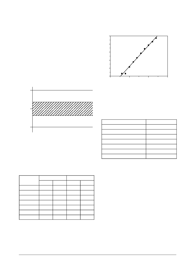
Results
An example of using a log MTBF versus
determine is shown in Figure 11.
t plot to
DELAY (SEC)
2
0
2
4
6
8
4e9
5e9
2e9
3e9
Figure 11. Plot of Log MTBF versus Delay
L
From Equation 4 the slope of the line is the reciprocal of
. Measurements similar to these were performed to
characterize the ECLinPS family as well as D flip
flops
from various vendors. The results are shown in Table 2:
Table 2. Values for Several Flip
Flops
Device Type
ON Semiconductor MC10E431
125 psec
ON Semiconductor MC10E151
185 psec
ON Semiconductor MC10E131
200 psec
ON Semiconductor MC10H131
718 psec
Signetics 100131
890 psec
Signetics 100151
1172 psec
National 100131
Having determined the value of , the system designer can
use this information in conjunction with Equation 3 to aid in
optimizing the system design.
Example
As an example, assume the system configuration shown
in Figure 12, in which the output from System 1 is to be
synchronized to System 2 using a 10E151 D flip
flop.
Further, the equivalent output signal for System 1 is
75 MHz whereas the clock frequency for System 2, as well
as the synchronizing element, is 100 MHz. Under these
conditions the data and clock inputs to the D flip
flop are
asynchronous and the system designer must consider the
possibility of the D flip
flop entering the metastable state.
Therefore the system designer must determine how long the
flip
flop will remain in the metastable region in order to
decide when the data at the output of the flip
flop will attain
a defined state and can be clocked into System 2.
The solution to this dilemma is found with Equation 3:
1594 psec
MTBF
1 (2 * fC* fD* TP* 10
( t)
)
(eq. 5)
相關(guān)PDF資料 |
PDF描述 |
|---|---|
| AN1568 | Interfacing Between LVDS and ECL |
| AN1568D | Interfacing Between LVDS and ECL |
| AN1593 | LOW COST 1.0 A CURRENT SOURCE FOR BATTERY CHARGERS |
| AN1607 | ITC122 low voltage micro to motor interface |
| AN1672 | The ECL Translator Guide |
相關(guān)代理商/技術(shù)參數(shù) |
參數(shù)描述 |
|---|---|
| AN15167A-VT | 制造商:Panasonic Industrial Company 功能描述:IC |
| AN1523 | 制造商:STMICROELECTRONICS 制造商全稱:STMicroelectronics 功能描述:11W FLYBACK CONVERTER FOR AUXILIARY POWER SUPPLY APPLICATION USING THE L6590 |
| AN1527 | 制造商:STMICROELECTRONICS 制造商全稱:STMicroelectronics 功能描述:DEVELOPING A USB SMARTCARD READER WITH ST7SCR |
| AN1549.0 | 制造商:INTERSIL 制造商全稱:Intersil Corporation 功能描述:Addressing Power Issues in Real Time Clock Applications |
| AN155 | 制造商:SILABS 制造商全稱:SILABS 功能描述:STEPPER MOTOR REFERENCE DESIGN |
發(fā)布緊急采購,3分鐘左右您將得到回復(fù)。