- 您現(xiàn)在的位置:買賣IC網(wǎng) > PDF目錄366544 > AM50DL128BH85I (Advanced Micro Devices, Inc.) Stacked Multi-Chip Package (MCP) Flash Memory and SRAM PDF資料下載
參數(shù)資料
| 型號: | AM50DL128BH85I |
| 廠商: | Advanced Micro Devices, Inc. |
| 元件分類: | SRAM |
| 英文描述: | Stacked Multi-Chip Package (MCP) Flash Memory and SRAM |
| 中文描述: | 堆疊式多芯片封裝(MCP)閃存和SRAM |
| 文件頁數(shù): | 31/68頁 |
| 文件大?。?/td> | 959K |
| 代理商: | AM50DL128BH85I |
第1頁第2頁第3頁第4頁第5頁第6頁第7頁第8頁第9頁第10頁第11頁第12頁第13頁第14頁第15頁第16頁第17頁第18頁第19頁第20頁第21頁第22頁第23頁第24頁第25頁第26頁第27頁第28頁第29頁第30頁當(dāng)前第31頁第32頁第33頁第34頁第35頁第36頁第37頁第38頁第39頁第40頁第41頁第42頁第43頁第44頁第45頁第46頁第47頁第48頁第49頁第50頁第51頁第52頁第53頁第54頁第55頁第56頁第57頁第58頁第59頁第60頁第61頁第62頁第63頁第64頁第65頁第66頁第67頁第68頁
October 7, 2003
Am50DL128BH
29
A D V A N C E I N F O R M A T I O N
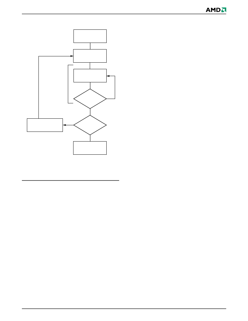
Figure 4.
Program Operation
Chip Erase Command Sequence
Chip erase is a six bus cycle operation. The chip erase
command sequence is initiated by writing two unlock
cycles, followed by a set-up command. Two additional
unlock write cycles are then followed by the chip erase
command, which in turn invokes the Embedded Erase
algorithm. The device does
not
require the system to
preprogram prior to erase. The Embedded Erase algo-
rithm automatically preprograms and verifies the entire
memory for an all zero data pattern prior to electrical
erase. The system is not required to provide any con-
trols or timings during these operations. Table 12
shows the address and data requirements for the chip
erase command sequence.
Note that the SecSi Sec-
tor, autoselect, and CFI functions are unavailable
when a erase operation is in progress.
When the Embedded Erase algorithm is complete,
that bank returns to the read mode and addresses are
no longer latched. The system can determine the sta-
tus of the erase operation by using DQ7, DQ6, DQ2,
or RY/BY#. Refer to the Flash Write Operation Status
section for information on these status bits.
Any commands written during the chip erase operation
are ignored. However, note that a
hardware reset
im-
mediately terminates the erase operation. If that oc-
curs, the chip erase command sequence should be
reinitiated once that bank has returned to reading
array data, to ensure data integrity.
Figure 5 illustrates the algorithm for the erase opera-
tion. Refer to the Erase and Program Operations ta-
bles in the AC Characteristics section for parameters,
and Figure 21 section for timing diagrams.
Sector Erase Command Sequence
Sector erase is a six bus cycle operation. The sector
erase command sequence is initiated by writing two
unlock cycles, followed by a set-up command. Two ad-
ditional unlock cycles are written, and are then fol-
lowed by the address of the sector to be erased, and
the sector erase command. Table 12 shows the ad-
dress and data requirements for the sector erase com-
mand sequence.
The device does
not
require the system to preprogram
prior to erase. The Embedded Erase algorithm auto-
matically programs and verifies the entire memory for
an all zero data pattern prior to electrical erase. The
system is not required to provide any controls or tim-
ings during these operations.
After the command sequence is written, a sector erase
time-out of 80 μs occurs. During the time-out period,
additional sector addresses and sector erase com-
mands may be written. Loading the sector erase buffer
may be done in any sequence, and the number of sec-
tors may be from one sector to all sectors. The time
between these additional cycles must be less than 80
μs, otherwise erasure may begin. Any sector erase
address and command following the exceeded
time-out may or may not be accepted. It is recom-
mended that processor interrupts be disabled during
this time to ensure all commands are accepted. The
interrupts can be re-enabled after the last Sector
Erase command is written.
Any command other than
Sector Erase or Erase Suspend during the
time-out period resets that bank to the read mode.
The system must rewrite the command sequence and
any additional addresses and commands.
Note that
the SecSi Sector, autoselect, and CFI functions are
unavailable when a erase operation is in progress.
The system can monitor DQ3 to determine if the sec-
tor erase timer has timed out (See the section on DQ3:
Sector Erase Timer.). The time-out begins from the ris-
ing edge of the final WE# pulse in the command
sequence.
When the Embedded Erase algorithm is complete, the
bank returns to reading array data and addresses are
no longer latched. Note that while the Embedded
Erase operation is in progress, the system can read
START
Write Program
Command Sequence
Data Poll
from System
Verify Data
No
Yes
Last Address
No
Yes
Programming
Completed
Increment Address
Embedded
Program
algorithm
in progress
Note:
See Table 12 for program command sequence.
相關(guān)PDF資料 |
PDF描述 |
|---|---|
| AM50DL128BH85IS | Stacked Multi-Chip Package (MCP) Flash Memory and SRAM |
| AM50DL128CG70IS | 64 Megabit (4 M x 16-Bit) CMOS 3.0 Volt-only, Simultaneous Operation Flash Memories and 64 Mbit (4 M x 16-Bit) Pseudo Static RAM |
| AM50DL128CG70IT | 64 Megabit (4 M x 16-Bit) CMOS 3.0 Volt-only, Simultaneous Operation Flash Memories and 64 Mbit (4 M x 16-Bit) Pseudo Static RAM |
| AM50DL128CG85IS | 64 Megabit (4 M x 16-Bit) CMOS 3.0 Volt-only, Simultaneous Operation Flash Memories and 64 Mbit (4 M x 16-Bit) Pseudo Static RAM |
| AM50DL128CG85IT | 64 Megabit (4 M x 16-Bit) CMOS 3.0 Volt-only, Simultaneous Operation Flash Memories and 64 Mbit (4 M x 16-Bit) Pseudo Static RAM |
相關(guān)代理商/技術(shù)參數(shù) |
參數(shù)描述 |
|---|---|
| AM50DL128BH85IS | 制造商:SPANSION 制造商全稱:SPANSION 功能描述:Two Am29DL640G 64 Megabit (8 M x 8-Bit/4 M x 16-Bit) CMOS 3.0 Volt-only, Simultaneous Operation Flash Memories |
| AM50DL128BH85IT | 制造商:SPANSION 制造商全稱:SPANSION 功能描述:Two Am29DL640G 64 Megabit (8 M x 8-Bit/4 M x 16-Bit) CMOS 3.0 Volt-only, Simultaneous Operation Flash Memories |
| AM50DL128CG | 制造商:SPANSION 制造商全稱:SPANSION 功能描述:Stacked Multi-Chip Package (MCP) Flash Memory and SRAM |
| AM50DL128CG70IS | 制造商:SPANSION 制造商全稱:SPANSION 功能描述:Stacked Multi-Chip Package (MCP) Flash Memory and SRAM |
| AM50DL128CG70IT | 制造商:SPANSION 制造商全稱:SPANSION 功能描述:Stacked Multi-Chip Package (MCP) Flash Memory and SRAM |
發(fā)布緊急采購,3分鐘左右您將得到回復(fù)。