- 您現(xiàn)在的位置:買賣IC網(wǎng) > PDF目錄366537 > AM30LV0064DJ40F2IT (ADVANCED MICRO DEVICES INC) 64 Megabit (8 M x 8-Bit) CMOS 3.0 Volt-only Flash Memory with UltraNAND Technology PDF資料下載
參數(shù)資料
| 型號(hào): | AM30LV0064DJ40F2IT |
| 廠商: | ADVANCED MICRO DEVICES INC |
| 元件分類: | PROM |
| 英文描述: | 64 Megabit (8 M x 8-Bit) CMOS 3.0 Volt-only Flash Memory with UltraNAND Technology |
| 中文描述: | 8M X 8 FLASH 3V PROM, 35 ns, PDSO40 |
| 封裝: | REVERSE, MO-024AC, TSOP2-44/40 |
| 文件頁數(shù): | 18/41頁 |
| 文件大?。?/td> | 1067K |
| 代理商: | AM30LV0064DJ40F2IT |
第1頁第2頁第3頁第4頁第5頁第6頁第7頁第8頁第9頁第10頁第11頁第12頁第13頁第14頁第15頁第16頁第17頁當(dāng)前第18頁第19頁第20頁第21頁第22頁第23頁第24頁第25頁第26頁第27頁第28頁第29頁第30頁第31頁第32頁第33頁第34頁第35頁第36頁第37頁第38頁第39頁第40頁第41頁
18
Am30LV0064D
Read Spare Area (50h)
The Read Spare Area command is similar to the Read
Data command, except that it only reads information
from the selected page 16 byte Spare Area (address
locations 512 through 527). After the command cycle
is used to write the Read Spare Area op-code to the
device, three address cycles are used to input the
starting address for the read operation. During the
Read Spare Area command cycle the SE# input must
be low.
Because the Read Spare Area operation only reads
the 16 byte spare area in the page, address bits
A7–A4 are don’t care. Address bits A22–A9 are used
to select the Page, and address bits A3–A0 are used
to select the starting byte within the Spare Area of the
Page. Upon the rising edge of the final WE# pulse
there is a 7 μs latency in which all 528 bytes of infor-
mation are transferred from the Flash array page to
the 528 byte Data Register. Following the data transfer
the internal address pointer will point to the byte se-
lected in the Spare Area. During the 7 μs data transfer
period the device will appear busy and the RY/BY#
signal or the status register may be used to monitor
the completion of the data transfer. Only the Reset and
Read Status commands are valid during the period
that the device is busy. Once the information has been
loaded into the Data Register, the Spare Area informa-
tion may be sequentially read with consecutive 50 ns
RE# pulses. Each RE# pulse will automatically ad-
vance the Spare Area column address by one. Once
the last column has been read, the page address will
automatically increment by one and the Data Register
will be updated with the new page after a 7 μs latency.
During the sequential read mode, the Spare Area En-
able input (SE#) must be low. This is necessary any
time the Spare Area is being read. In this operation,
the column address will advance from the selected
starting byte location to address 527 before the page
address is incremented. After the next page of infor-
mation is transferred to the Data Register, sequential
read operations will begin in the Data Register at ad-
dress location 512. Unlike the Read Data and Gapless
Read modes, the Read Spare Area operation requires
that the SE# input be asserted low prior to the com-
mand being issued to the device.
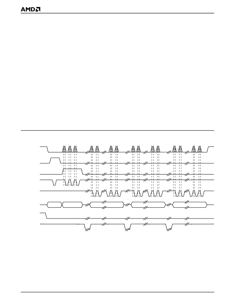
Figure 4. Read Spare Area
CE#
CLE
ALE
WE#
RE#
I/O7-0
SE#
RY/BY#
CMD
Start Address
Read Spare Area
Read Next Spare Area
Read Next Spare Area
Data Transfer
Data Transfer
Data Transfer
Read Spare Area (50h)
相關(guān)PDF資料 |
PDF描述 |
|---|---|
| AM30LV0064DJ40WGIT | 64 Megabit (8 M x 8-Bit) CMOS 3.0 Volt-only Flash Memory with UltraNAND Technology |
| AM33C93A | LJT 16C 16#16 SKT RECP |
| AM3F-1205SH30 | 3 watt dc-dc converters |
| AM3F | 3 watt dc-dc converters |
| AM3F-0503S | 3 watt dc-dc converters |
相關(guān)代理商/技術(shù)參數(shù) |
參數(shù)描述 |
|---|---|
| AM30LV0064DJ40WGI | 制造商:未知廠家 制造商全稱:未知廠家 功能描述:NAND Flash EEPROM |
| AM30LV0064DJ40WGIT | 制造商:AMD 制造商全稱:Advanced Micro Devices 功能描述:64 Megabit (8 M x 8-Bit) CMOS 3.0 Volt-only Flash Memory with UltraNAND Technology |
| AM30N02-40D | 制造商:ANALOGPOWER 制造商全稱:ANALOGPOWER 功能描述:N-Channel 20-V (D-S) MOSFET |
| AM30N02-59D | 制造商:ANALOGPOWER 制造商全稱:ANALOGPOWER 功能描述:N-Channel 20-V (D-S) MOSFET |
| AM30N03-40D | 制造商:ANALOGPOWER 制造商全稱:ANALOGPOWER 功能描述:N-Channel 30-V (D-S) MOSFET |
發(fā)布緊急采購(gòu),3分鐘左右您將得到回復(fù)。