- 您現(xiàn)在的位置:買賣IC網(wǎng) > PDF目錄362243 > AM29F200B-120FI 150V Single N-Channel Digital Audio HEXFET Power MOSFET in a TO-220AB package; A IRFB4019PBF with Standard Packaging PDF資料下載
參數(shù)資料
| 型號: | AM29F200B-120FI |
| 英文描述: | 150V Single N-Channel Digital Audio HEXFET Power MOSFET in a TO-220AB package; A IRFB4019PBF with Standard Packaging |
| 中文描述: | x8/x16閃存EEPROM |
| 文件頁數(shù): | 8/39頁 |
| 文件大小: | 728K |
| 代理商: | AM29F200B-120FI |
第1頁第2頁第3頁第4頁第5頁第6頁第7頁當前第8頁第9頁第10頁第11頁第12頁第13頁第14頁第15頁第16頁第17頁第18頁第19頁第20頁第21頁第22頁第23頁第24頁第25頁第26頁第27頁第28頁第29頁第30頁第31頁第32頁第33頁第34頁第35頁第36頁第37頁第38頁第39頁
8
Am29F002B/Am29F002NB
DEVICE BUS OPERATIONS
This section describes the requirements and use of the
device bus operations, which are initiated through the
internal command register. The command register
itself does not occupy any addressable memory loca-
tion. The register is composed of latches that store the
commands, along with the address and data informa-
tion needed to execute the command. The contents of
the register serve as inputs to the internal state
machine. The state machine outputs dictate the func-
tion of the device. The appropriate device bus
operations table lists the inputs and control levels
required, and the resulting output. The following sub-
sections describe each of these operations in further
detail.
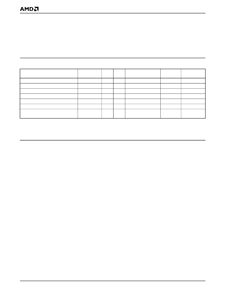
Table 1.
Am29F002B/Am29F002NB Device Bus Operations
Legend:
L = Logic Low = VIL, H = Logic High = VIH, VID = 12.0 ± 0.5 V, X = Don’t Care, DIN = Data In, DOUT = Data Out, A
IN
= Address In
Note:
See the sections on Sector Group Protection and Temporary Sector Unprotect for more information. This function requires
the RESET# pin and is therefore not available on the Am29F002NB device.
Requirements for Reading Array Data
To read array data from the outputs, the system must
drive the CE# and OE# pins to V
IL
. CE# is the power
control and selects the device. OE# is the output
control and gates array data to the output pins. WE#
should remain at V
IH
.
The internal state machine is set for reading array data
upon device power-up, or after a hardware reset. This
ensures that no spurious alteration of the memory
content occurs during the power transition. No
command is necessary in this mode to obtain array
data. Standard microprocessor read cycles that assert
valid addresses on the device address inputs produce
valid data on the device data outputs. The device
remains enabled for read access until the command
register contents are altered.
See “Reading Array Data” for more information. Refer
to the AC Read Operations table for timing specifica-
tions and to the Read Operations Timings diagram for
the timing waveforms. I
CC1
in the DC Characteristics
table represents the active current specification for
reading array data.
Writing Commands/Command Sequences
To write a command or command sequence (which
includes programming data to the device and erasing
sectors of memory), the system must drive WE# and
CE# to V
IL
, and OE# to V
IH
.
An erase operation can erase one sector, multiple sec-
tors, or the entire device. The Sector Address Tables
indicate the address space that each sector occupies.
A “sector address” consists of the address bits required
to uniquely select a sector. See the Command Defini-
tions section for details on erasing a sector or the entire
chip, or suspending/resuming the erase operation.
After the system writes the autoselect command
sequence, the device enters the autoselect mode. The
system can then read autoselect codes from the
internal register (which is separate from the memory
array) on DQ7–DQ0. Standard read cycle timings apply
in this mode. Refer to the “Autoselect Mode” and
Autoselect Command Sequence sections for more
information.
I
CC2
in the DC Characteristics table represents the
active current specification for the write mode. The “AC
Characteristics” section contains timing specification
tables and timing diagrams for write operations.
Program and Erase Operation Status
During an erase or program operation, the system may
check the status of the operation by reading the status
bits on DQ7–DQ0. Standard read cycle timings and I
CC
read specifications apply. Refer to “Write Operation
Operation
CE#
L
L
OE#
L
H
X
X
H
X
WE#
H
L
X
X
H
X
RESET#
(n/a Am29F002NB)
H
H
H
H
H
L
A0–A17
A
IN
A
IN
X
X
X
X
DQ0–DQ7
D
OUT
D
IN
High-Z
High-Z
High-Z
High-Z
Read
Write
CMOS Standby
TTL Standby
Output Disable
Reset (n/a on Am29F002NB)
Temporary Sector Unprotect
(See Note)
V
CC
± 0.5 V
H
L
X
X
X
X
V
ID
X
X
相關(guān)PDF資料 |
PDF描述 |
|---|---|
| AM29F200B-120SC | x8/x16 Flash EEPROM |
| AM29F200B-120SE | x8/x16 Flash EEPROM |
| AM29F200B-120SEB | x8/x16 Flash EEPROM |
| AM29F200B-120SI | 12V Single N-Channel HEXFET Power MOSFET in a SO-8 package; Similar to IRF7476 with Lead Free Packaging |
| AM29F200B-150EC | 30V Single N-Channel HEXFET Power MOSFET in a SO-8 package; Similar to IRF7807A with Lead Free Packaging |
相關(guān)代理商/技術(shù)參數(shù) |
參數(shù)描述 |
|---|---|
| AM29F200BB-120EC | 制造商:Advanced Micro Devices 功能描述: |
| AM29F200BB-120SI | 制造商:Spansion 功能描述:NOR Flash Parallel 5V 2Mbit 256K/128K x 8bit/16bit 120ns 44-Pin SOIC |
| AM29F200BB-120SI\T | 制造商:Spansion 功能描述:Flash Mem Parallel 5V 2M-Bit 256K x 8/128K x 16 120ns 44-Pin SOIC T/R |
| AM29F200BB-45SI | 制造商:Advanced Micro Devices 功能描述: |
| AM29F200BB-55EF | 功能描述:閃存 2M (256KX8/128KX16) Parallel NOR Fl 5V RoHS:否 制造商:ON Semiconductor 數(shù)據(jù)總線寬度:1 bit 存儲類型:Flash 存儲容量:2 MB 結(jié)構(gòu):256 K x 8 定時類型: 接口類型:SPI 訪問時間: 電源電壓-最大:3.6 V 電源電壓-最小:2.3 V 最大工作電流:15 mA 工作溫度:- 40 C to + 85 C 安裝風(fēng)格:SMD/SMT 封裝 / 箱體: 封裝:Reel |
發(fā)布緊急采購,3分鐘左右您將得到回復(fù)。