- 您現(xiàn)在的位置:買賣IC網(wǎng) > PDF目錄36682 > AGR21125EF (LSI CORP) S BAND, Si, N-CHANNEL, RF POWER, MOSFET PDF資料下載
參數(shù)資料
| 型號: | AGR21125EF |
| 廠商: | LSI CORP |
| 元件分類: | 功率晶體管 |
| 英文描述: | S BAND, Si, N-CHANNEL, RF POWER, MOSFET |
| 封裝: | FM-2 |
| 文件頁數(shù): | 1/10頁 |
| 文件大小: | 217K |
| 代理商: | AGR21125EF |
Preliminary Data Sheet
April 2004
AGR21125E
125 W, 2.110 GHz—2.170 GHz, N-Channel E-Mode, Lateral MOSFET
Introduction
The AGR21125E is a high-voltage, gold-metalized,
enhancement mode, laterally diffused metal oxide
semiconductor (LDMOS) RF power transistor suit-
able for wideband code division multiple access
(W-CDMA), single and multicarrier class AB wireless
base station power amplifier applications.
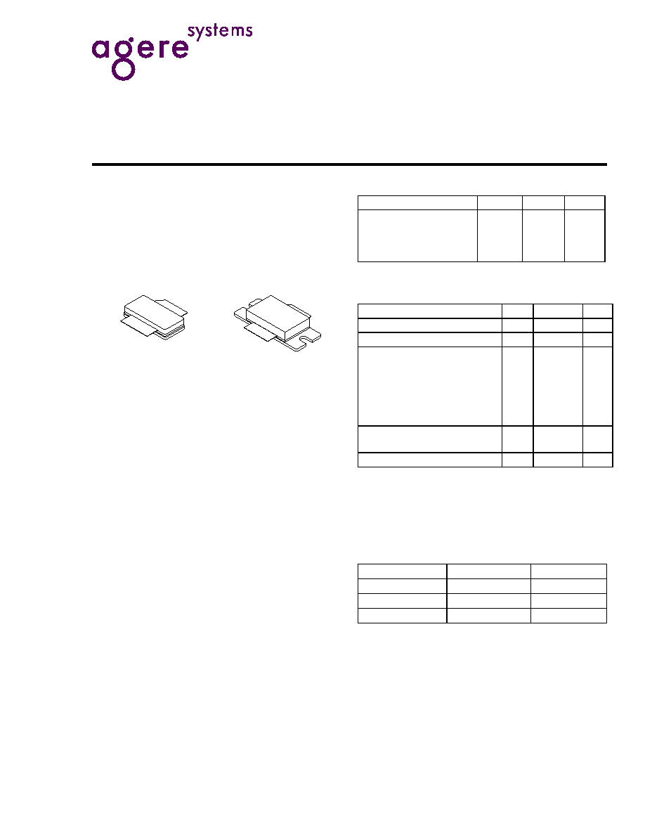
Figure 1. Available Packages
Features
s
Typical performance for two carrier 3GPP
W-CDMA systems. F1 = 2135 MHz and
F2 = 2145 MHz with 3.84 MHz channel BW, adja-
cent channel BW = 3.84 MHz at F1 – 5 MHz and
F2 + 5 MHz. Third-order distortion is measured
over 3.84 MHz BW at F1 – 10 MHz and
F2 + 10 MHz. Typical P/A ratio of 8.5 dB at 0.01%
(probability) CCDF:
— Output power: 28 W.
— Power gain: 14 dB.
— Efficiency: 27%.
— IM3: –34.5 dBc.
— ACPR: –38 dBc.
— Return loss: –10 dB.
s
High-reliability, gold-metalization process.
s
Low hot carrier injection (HCI) induced bias drift
over 20 years.
s
Internally matched.
s
High gain, efficiency, and linearity.
s
Integrated ESD protection.
s
Device can withstand a 10:1 voltage standing wave
ratio (VSWR) at 28 Vdc, 2140 MHz, 125 W contin-
uous wave (CW) output power.
s
Large signal impedance parameters available.
Table 1. Thermal Characteristics
Table 2. Absolute Maximum Ratings*
* Stresses in excess of the absolute maximum ratings can cause
permanent damage to the device. These are absolute stress rat-
ings only. Functional operation of the device is not implied at
these or any other conditions in excess of those given in the
operational sections of the data sheet. Exposure to absolute
maximum ratings for extended periods can adversely affect
device reliability.
Table 3. ESD Rating*
* Although electrostatic discharge (ESD) protection circuitry has
been designed into this device, proper precautions must be
taken to avoid exposure to ESD and electrical overstress (EOS)
during all handling, assembly, and test operations. Agere
employs a human-body model (HBM), a machine model (MM),
and a charged-device model (CDM) qualification requirement in
order to determine ESD-susceptibility limits and protection
design evaluation. ESD voltage thresholds are dependent on the
circuit parameters used in each of the models, as defined by
JEDEC's JESD22-A114B (HBM), JESD22-A115A (MM), and
JESD22-C101A (CDM) standards.
Caution: MOS devices are susceptible to damage from elec-
trostatic charge. Reasonable precautions in han-
dling and packaging MOS devices should be
observed.
AGR21125EU (unflanged)
AGR21125EF (flanged)
)
5B 03 STYLE 1
Parameter
Sym
Value
Unit
Thermal Resistance,
Junction to Case:
AGR21125EU
AGR21125EF
R
θJC
R
θJC
0.5
°C/W
Parameter
Sym
Value
Unit
Drain-source Voltage
VDSS
65
Vdc
Gate-source Voltage
VGS –0.5, +15 Vdc
Total Dissipation at TC = 25 °C:
AGR21125EU
AGR21125EF
PD
350
W
Derate Above 25
°C:
AGR21125EU
AGR21125EF
—
2.0
W/°C
Operating Junction Tempera-
ture
TJ
200
°C
Storage Temperature Range
TSTG –65, +150
°C
AGR21125E
Minimum (V)
Class
HBM
500
1B
MM
50
A
CDM
1500
4
相關(guān)PDF資料 |
PDF描述 |
|---|---|
| AGR26045EF | UHF BAND, Si, N-CHANNEL, RF POWER, MOSFET |
| AGR26045EF | UHF BAND, Si, N-CHANNEL, RF POWER, MOSFET |
| AGR26125EU | S BAND, Si, N-CHANNEL, RF POWER, MOSFET |
| AGR26180EF | UHF BAND, Si, N-CHANNEL, RF POWER, MOSFET |
| AGR26180EF | UHF BAND, Si, N-CHANNEL, RF POWER, MOSFET |
相關(guān)代理商/技術(shù)參數(shù) |
參數(shù)描述 |
|---|---|
| AGR21125EU | 制造商:TRIQUINT 制造商全稱:TriQuint Semiconductor 功能描述:125 W, 2.110 GHz-2.170 GHz, N-Channel E-Mode, Lateral MOSFET |
| AGR21180EF | 功能描述:射頻MOSFET電源晶體管 RF Transistor RoHS:否 制造商:Freescale Semiconductor 配置:Single 晶體管極性: 頻率:1800 MHz to 2000 MHz 增益:27 dB 輸出功率:100 W 汲極/源極擊穿電壓: 漏極連續(xù)電流: 閘/源擊穿電壓: 最大工作溫度: 封裝 / 箱體:NI-780-4 封裝:Tray |
| AGR21N090EF | 功能描述:射頻MOSFET電源晶體管 RF Transistor RoHS:否 制造商:Freescale Semiconductor 配置:Single 晶體管極性: 頻率:1800 MHz to 2000 MHz 增益:27 dB 輸出功率:100 W 汲極/源極擊穿電壓: 漏極連續(xù)電流: 閘/源擊穿電壓: 最大工作溫度: 封裝 / 箱體:NI-780-4 封裝:Tray |
| AGR26045EF | 功能描述:射頻MOSFET電源晶體管 RF Transistor RoHS:否 制造商:Freescale Semiconductor 配置:Single 晶體管極性: 頻率:1800 MHz to 2000 MHz 增益:27 dB 輸出功率:100 W 汲極/源極擊穿電壓: 漏極連續(xù)電流: 閘/源擊穿電壓: 最大工作溫度: 封裝 / 箱體:NI-780-4 封裝:Tray |
| AGR26125E | 制造商:TRIQUINT 制造商全稱:TriQuint Semiconductor 功能描述:125 W, 2.5 GHz-2.7 GHz, N-Channel E-Mode, Lateral MOSFET |
發(fā)布緊急采購,3分鐘左右您將得到回復(fù)。